Preparation method of bonding mark, wafer bonding method, bonding mark and semiconductor device

A wafer bonding and marking technology, used in semiconductor devices, semiconductor/solid-state device manufacturing, semiconductor/solid-state device components, etc., can solve problems such as bonding void risks, and achieve the effect of improving bonding quality and identification.

Pending Publication Date: 2020-02-28
SHANGHAI HUALI MICROELECTRONICS CORP
View PDF10 Cites 1 Cited by
  • Summary
  • Abstract
  • Description
  • Claims
  • Application Information

AI Technical Summary

Problems solved by technology

[0007] The purpose of the present invention is to provide a method for preparing a bonding mark to imp...

Method used


Image

  • Preparation method of bonding mark, wafer bonding method, bonding mark and semiconductor device
  • Preparation method of bonding mark, wafer bonding method, bonding mark and semiconductor device
  • Preparation method of bonding mark, wafer bonding method, bonding mark and semiconductor device

Examples


Embodiment Construction

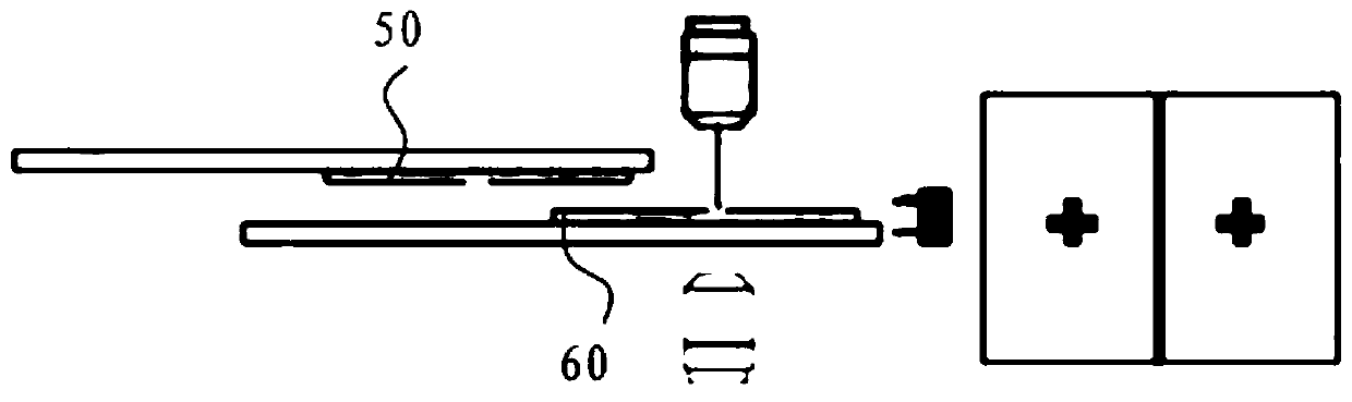
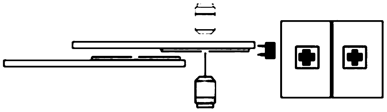
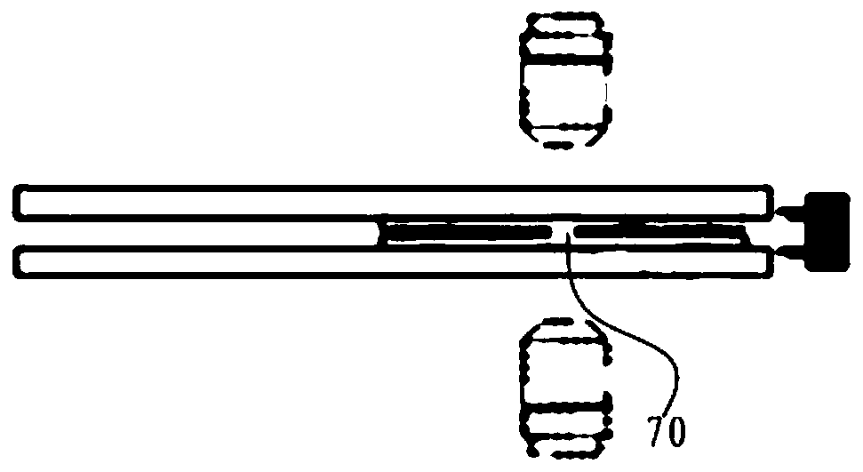
[0039] Figures 1A-1C For the process of wafer bonding alignment, first use the upper target to locate the position of the mark on the lower wafer 60 (i.e. the device wafer), digitally image and save the position; then use the lower target to adjust the upper wafer 50 (i.e. the carrier wafer) and digitally image it; finally restore the position of the lower wafer 60 and contact the upper wafer 50 to form overlay alignment marks 70 .

[0040] The process flow of wafer bonding is as follows: figure 2 with 3 As shown, first, a dry etching process is used on the carrier wafer (ie, the upper wafer) to etch a groove with a depth of 100nm as a bonding mark (ie, the upper wafer is used for bonding alignment and alignment testing. alignment marks). The carrier wafer is preferably a silicon wafer, and may include a silicon substrate 20 and a pad oxide layer 10 thereon, that is, a trench with a depth of 100 nm is etched on the pad oxide layer 10 and the silicon substrate 20 by dry etc...


PUM


Abstract

The invention provides a preparation method of a bonding mark. The method comprises steps of S1, forming a groove on a bearing wafer through etching; S2, filling metal in the groove; and S3, removingthe metal on a surface of the bearing wafer to retain the metal filled in the groove so as to form a bonding mark on the bearing wafer. The preparation method is advantaged in that after the groove isformed by etching, identification of the surface of the mark is improved by depositing metal in the groove, the risk of a bonding gap caused by the groove is reduced, and the bonding quality is improved. Furthermore, the invention further provides a bonding mark prepared based on the method, and the bonding mark has a clear boundary and is easy to identify, the identification failure rate is reduced, the wafer rejection rate can be reduced, and productivity is improved. Furthermore, the invention further provides a wafer bonding method and a semiconductor device prepared based on the wafer bonding method.

Description

technical field [0001] The invention belongs to the field of semiconductors, and in particular relates to a method for preparing a bonding mark, a wafer bonding method, a bonding mark and a semiconductor device. Background technique [0002] With the rapid development of semiconductor technology, Complementary Metal Oxide Semiconductor (CMOS for short) and Micro Electro Mechanical Systems (MEMS for short) devices have become the most mainstream technology in the market of various sensor products, and With the continuous advancement of technology, such products will develop in the direction of smaller size, higher electrical performance and lower loss. [0003] The CMOS image sensor is the core component of camera equipment, which realizes the image capture function by converting optical signals into electrical signals. Because of its advantages of low power consumption and high signal-to-noise ratio, it has been widely used in various fields. [0004] Taking back-illuminat...

Claims


Application Information

Patent Timeline
IPC IPC(8): H01L21/68H01L23/544
CPCH01L21/682H01L23/544H01L2223/54426
Inventor 毛益平姬峰彭翔王奇伟陈昊瑜
Owner SHANGHAI HUALI MICROELECTRONICS CORP
Why Eureka
Try Eureka