Standard unit substrate-coupling capacitor layout structure based on FinFET technology

A standard cell, coupling capacitor technology, applied in the direction of capacitors, circuits, electrical components, etc., can solve the problem of dense and single source area arrangement, and achieve the effect of increasing the density of the active area

Active Publication Date: 2020-02-28
SHANGHAI HUALI INTEGRATED CIRCUTE MFG CO LTD
View PDF6 Cites 2 Cited by
  • Summary
  • Abstract
  • Description
  • Claims
  • Application Information

AI Technical Summary

Problems solved by technology

[0004] In view of the above-mentioned shortcomings of the prior art, the purpose of the present invention is to provide a standard cell substrate-coupling capacitor layout structure based on FinFET technology, which is used to solve the problem that can only be realized in the standard cell substrate layout structure in the prior art. A single substrate function, and the active area is densely arranged

Method used


Image

  • Standard unit substrate-coupling capacitor layout structure based on FinFET technology
  • Standard unit substrate-coupling capacitor layout structure based on FinFET technology
  • Standard unit substrate-coupling capacitor layout structure based on FinFET technology

Examples


Embodiment Construction

[0027] Embodiments of the present invention are described below through specific examples, and those skilled in the art can easily understand other advantages and effects of the present invention from the content disclosed in this specification. The present invention can also be implemented or applied through other different specific implementation modes, and various modifications or changes can be made to the details in this specification based on different viewpoints and applications without departing from the spirit of the present invention.

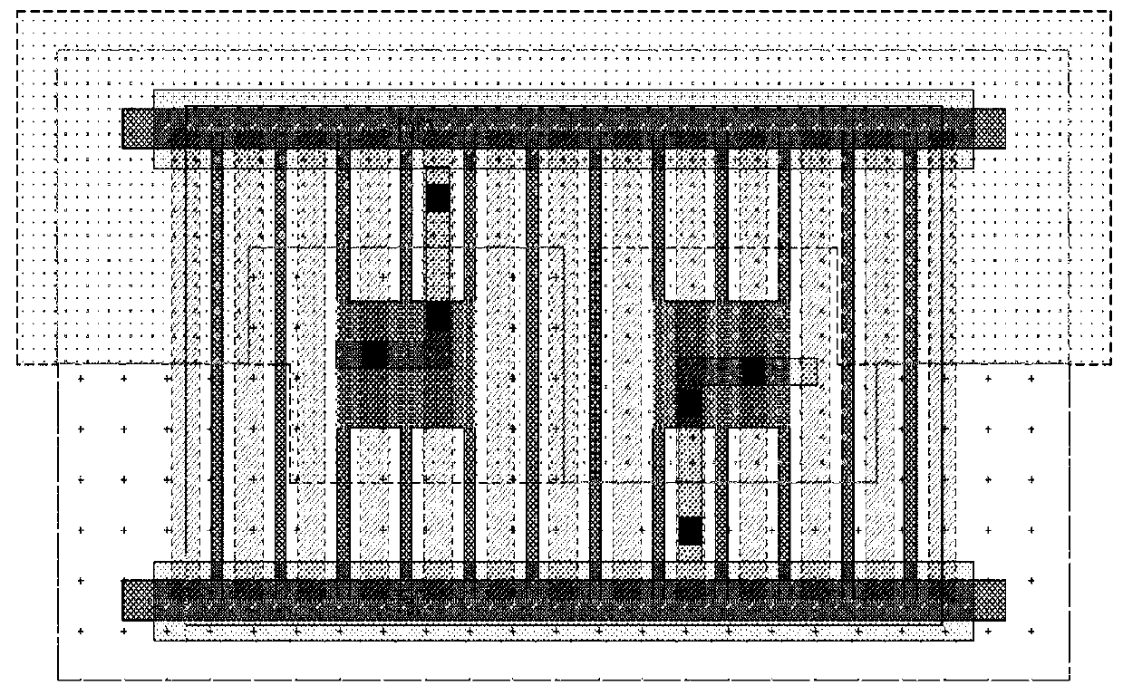
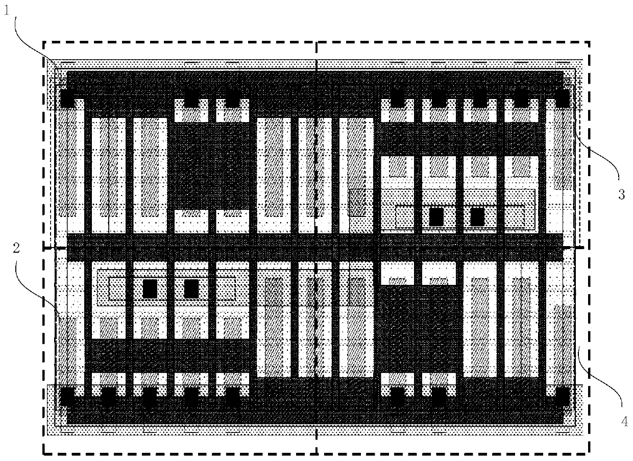
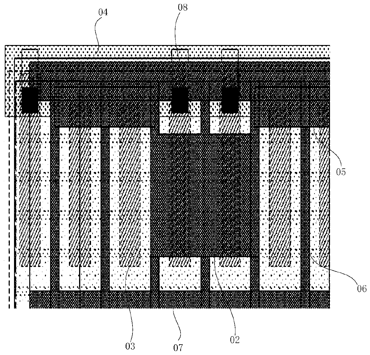
[0028] see Figure 2 to Figure 3d . It should be noted that the diagrams provided in this embodiment are only schematically illustrating the basic idea of ​​the present invention, and only the components related to the present invention are shown in the diagrams rather than the number, shape and shape of the components in actual implementation. Dimensional drawing, the type, quantity and proportion of each component can be changed ar...


PUM


Abstract

The invention provides a standard unit substrate-coupling capacitor layout structure based on a FinFET technology. The standard unit substrate-coupling capacitor layout structure is composed of a first layout area, a second layout area, a third layout area and a fourth layout area, and comprises an active region, a fin layer, a metal 0 layer, a contact hole layer, a metal 1 layer, a metal 0 layercut-off layer, a polycrystalline silicon layer, a polycrystalline silicon edge defining layer and a polycrystalline silicon cut-off layer, wherein the polycrystalline silicon layer is a plurality of strip-shaped structures which are arranged at equal intervals, the overlapping area of the polycrystalline silicon layer and the active region in the first layout region, the second layout region, thethird layout region and the fourth layout region is attached and surrounded by the polycrystalline silicon edge defining layer. On the basis that the original layout area is not increased, the densityof the active region is increased, and the dual functions of the substrate and the coupling capacitor are achieved at the same time.

Description

technical field [0001] The invention relates to the field of semiconductor manufacturing, in particular to a standard unit substrate-coupling capacitor layout structure based on FinFET technology. Background technique [0002] Such as figure 1 as shown, figure 1 It is shown as a standard cell TAP (substrate) layout in the prior art. The entire cell layout is 12 Poly Pitch (the sum of polysilicon line width and spacing) width, and the layout is divided into a first layout area and a second layout area. Wherein, the first layout area is NTAP (N-type substrate), and the second layout area is PTAP (P-type substrate). This layout can only realize the TAP (substrate) function alone, and the active area arrangement density (AA density) is low, which is prone to problems. [0003] Therefore, it is necessary to propose a new standard cell substrate-coupling capacitor layout structure based on FinFET technology to solve the above-mentioned problems of single function and low arrang...

Claims


Application Information

Patent Timeline
Patent Type & Authority Applications(China)
IPC IPC(8): H01L27/02H01L23/64
CPCH01L27/0207H01L28/40
Inventor 阳媛胡晓明
Owner SHANGHAI HUALI INTEGRATED CIRCUTE MFG CO LTD
Why Eureka
Try Eureka