Manufacturing method for patterned substrate, patterned substrate and light emitting diode

A technology for patterning substrates and light-emitting diodes, which is applied in semiconductor/solid-state device manufacturing, electrical components, circuits, etc., can solve the problems of slow substrate etching, increased process time for patterned substrates, and difficulty in eliminating by-products. , to reduce the etching height, increase the production capacity, and shorten the process time.

Active Publication Date: 2020-03-06
BEIJING NAURA MICROELECTRONICS EQUIP CO LTD
View PDF5 Cites 1 Cited by
  • Summary
  • Abstract
  • Description
  • Claims
  • Application Information

AI Technical Summary

Problems solved by technology

[0003] In the related art, the manufacturing method of PSS patterned substrate generally includes main etching and over etching. During the main etching process, the photoresist coated on the substrate is often relatively high, about 3.5 μm-3.8 μm , the bottom width is about 1.8 μm to 1.9 μm. In this way, due to the high photoresist, the by-products of PSS etching are difficult to exclude, resulting in slow substrate etching, which greatly increases the process time of patterned substrates.

Method used


Image

  • Manufacturing method for patterned substrate, patterned substrate and light emitting diode

Examples


Embodiment Construction

[0025] The specific embodiments of the present invention will be described in detail below with reference to the accompanying drawings. It should be understood that the specific embodiments described herein are only used to illustrate and explain the present invention, and not to limit the present invention.

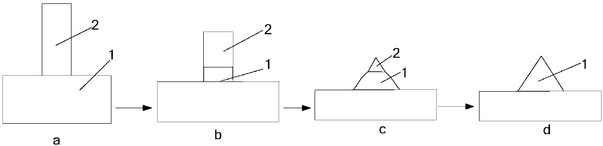
[0026] The first aspect of the present invention relates to a method for patterning a substrate, which includes a mask lowering stage, a main etching stage, and an over-etching stage in sequence.

[0027] Mask lowering stage: the substrate with the mask formed on the surface is etched with the preset first etching process parameters, and the first etching process parameters satisfy: the etching rate of the mask is greater than the etching rate of the substrate, To reduce the height of the mask.

[0028] Specifically, such as figure 1 As shown in the figure a, on the substrate 1 (the substrate 1 is generally a sapphire substrate, of course, other materials can also be selected...


PUM


Abstract

The invention discloses a method of patterning a substrate, the patterned substrate and a light emitting diode. The method comprises a mask lowering stage, a main etching stage and an over-etching stage which are carried out in sequence. In the mask lowering stage, a substrate with a mask formed on the surface is etched according to preset first etching process parameters, and the first etching process parameters meet that the etching rate of the mask is larger than that of the substrate so as to lower the height of the mask. In the main etching stage, the substrate subjected to the mask lowering stage is etched according to a preset second etching process parameter so as to improve the included angle between the bottom width and the inflection point of the substrate. In the over-etching stage, the morphology of the substrate subjected to the main etching stage is modified according to preset third etching process parameters to obtain a patterned substrate. According to the method of patterning the substrate, the process time can be effectively shortened, and the production capacity is improved.

Description

Technical field [0001] The invention relates to the technical field of semiconductor manufacturing, in particular to a manufacturing method of a patterned substrate, a patterned substrate and a light emitting diode. Background technique [0002] PSS (Patterned Sapphire Substrates) is a patterned substrate technology, which is a commonly used method to improve the light efficiency of GaN-based LED devices, that is, to grow a dry etching mask on a sapphire substrate, using standard light The etching process etches the mask into a pattern, etches the sapphire by using the ICP etching technique, removes the mask, and then grows GaN material on it, so that the vertical epitaxy of the GaN material becomes the horizontal epitaxy. This method can effectively reduce the dislocation density of the GaN epitaxial material, thereby reducing the non-radiative recombination of the active region, reducing the reverse leakage current, and improving the life of the LED. The light emitted from the...

Claims


Application Information

Patent Timeline
Patent Type & Authority Applications(China)
IPC IPC(8): H01L33/20H01L33/00H01L21/3065
CPCH01L21/3065H01L33/0075H01L33/20
Inventor 张君
Owner BEIJING NAURA MICROELECTRONICS EQUIP CO LTD
Why Eureka
Try Eureka