

Polishing treatment method of surface of back plate of target material
A processing method and target material technology, which is applied in the direction of grinding/polishing equipment, metal processing equipment, manufacturing tools, etc., can solve problems such as rust and burrs that are difficult to remove, low polishing efficiency, and sputtering target scrapping, etc., to achieve High industrial application value, uniform polishing texture, and improved polishing efficiency
- Summary
- Abstract
- Description
- Claims
- Application Information
AI Technical Summary
Problems solved by technology
Method used
Image

Examples
Embodiment 1
[0066] This embodiment provides a method for polishing the surface of a target back plate, the method comprising the following steps:
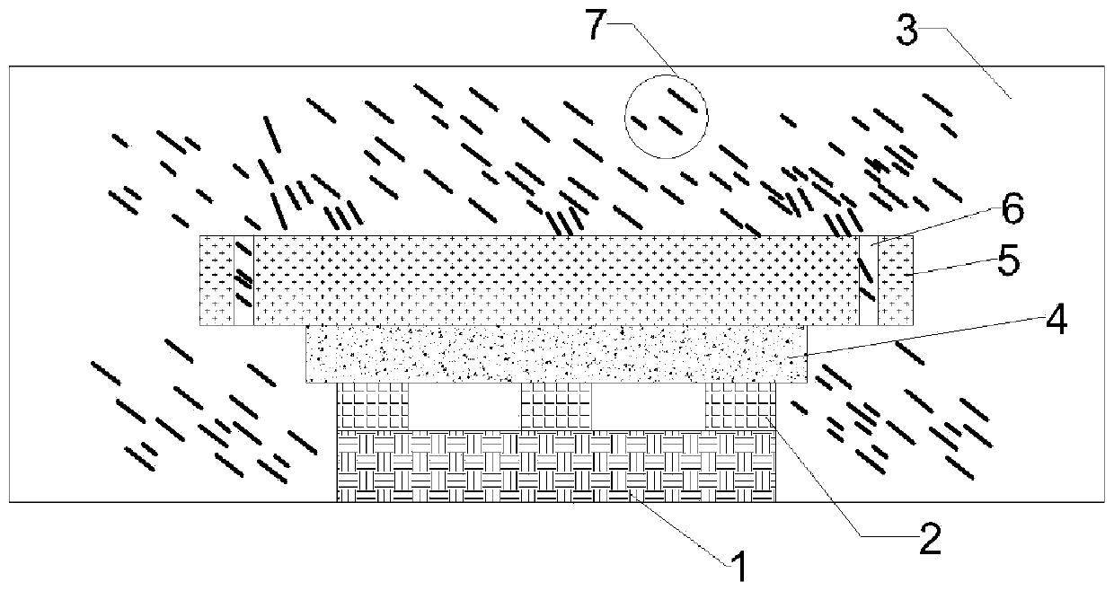
[0067] (1) The target assembly is placed upside down in the magnetic polishing machine, with the target back plate facing upwards, a 3cm high pad is placed below the target of the target assembly, and the target surface of the target assembly is covered with a cleaning cloth; Add the polishing solution in the magnetic polishing machine, the height of the polishing solution in the magnetic polishing machine is 4cm higher than the height of the target assembly, the polishing solution includes water, abrasive and carboxylic acid, the volume concentration of the abrasive in the polishing solution is 20%, and the volume concentration of carboxylic acid in the polishing solution is 10%; Add three kinds of grinding steel needles of different specifications in the magnetic polishing machine, and the diameters of the grinding steel needles of the three ...
Embodiment 2
[0070] This embodiment provides a method for polishing the surface of a target back plate, the method comprising the following steps:
[0071] (1) The target assembly is placed upside down in the magnetic polishing machine, with the target back plate facing upwards, a 2cm high pad is set below the target of the target assembly, and the target surface of the target assembly is covered with a cleaning cloth; First add water in the magnetic polishing machine, the height of the water in the magnetic polishing machine is 3cm higher than the height of the target assembly, then add abrasives in the magnetic polishing machine, and further add sulfur in the magnetic polishing machine acid, add four kinds of grinding steel needles of different specifications in the magnetic polishing machine, the diameters of the grinding steel needles of the four specifications are respectively 0.2mm, 0.5mm, 0.8mm and 1.0mm, and the lengths are respectively 1mm, 1.5 mm, 3.5mm and 4mm; the total volume ...
Embodiment 3
[0074] This embodiment provides a method for polishing the surface of a target back plate, the method comprising the following steps:
[0075] (1) Put the target assembly upside down in the magnetic polishing machine, with the target back plate facing up, and set a 4cm high pad under the target of the target assembly, and the target surface of the target assembly is covered with a target protection layer; add polishing solution in the magnetic polishing machine, the height of the polishing solution in the magnetic polishing machine is 5cm higher than the height of the target assembly, and the polishing solution includes water, abrasive, carboxylic acid and sulfonic acid, and the abrasive is polishing The volume concentration in the solution is 30%, and the volume concentration of carboxylic acid and sulfonic acid in the polishing solution is 15%; Add three kinds of grinding steel needles of different specifications in the magnetic polishing machine, and the grinding steel needl...
PUM
| Property | Measurement | Unit |
|---|---|---|
| height | aaaaa | aaaaa |
| diameter | aaaaa | aaaaa |
| diameter | aaaaa | aaaaa |
Abstract
Description
Claims
Application Information