Thin film thermal-sensitive printing head and manufacturing method thereof
A technology of thermal print head and manufacturing method, which is applied in printing and other directions, can solve the problems of high cost and slow welding speed of gold wire connecting IC and aluminum circuit, and achieve the effects of fast welding speed, high production efficiency and reduced production cost
- Summary
- Abstract
- Description
- Claims
- Application Information
AI Technical Summary
Problems solved by technology
Method used
Image

Examples
Embodiment 1
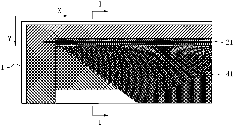
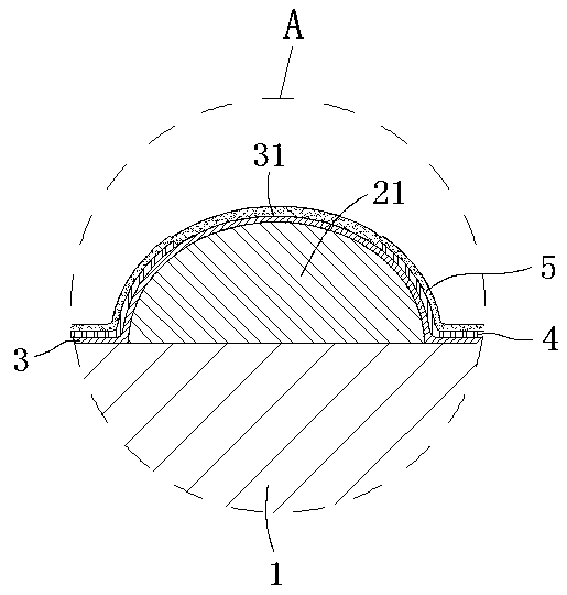
[0048] like Figure 1-5 As shown, a thin-film thermal print head includes a substrate 1, a thermal storage layer, a resistance layer 3, a conductive layer 4, a protective layer 5, an anti-oxidation layer 6, a driver IC 7 and a protective layer 8, and the substrate 1 is alumina ceramics plate.
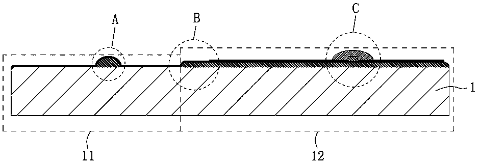
[0049] The substrate 1 is divided into adjacent first part 11 and second part 12 , the length direction of the substrate 1 is the X direction in the figure, and the width direction is the Y direction in the figure. The thermal storage layer includes a protruding portion 21 provided on the first part 11 of the substrate 1 and a base part 22 provided on the second part 12 of the substrate 1. The thermal storage layer is made of glass glaze with a thickness of 10um-500um.
[0050] The resistance layer 3 covers the outside of the substrate 1 and the heat storage layer. The resistance layer 3 has several heat generating parts 31 arranged at intervals along the length direction of the substr...
Embodiment 2
[0060] like Figure 6-9 As shown, the difference between this embodiment and the first embodiment is that the material of the conductive layer 4 is one of copper, tin, copper alloy, and tin alloy. A first connection layer 91 is provided between the conductive layer 4 and the resistance layer 3 , and a second connection layer 92 is provided between the protective layer 5 and the conductive layer 4 . The material of the first connection layer 91 and the second connection layer 92 is one of titanium, nickel, chromium, aluminum, titanium alloy, nickel alloy, chromium alloy, and aluminum alloy. Both the first connection layer 91 and the second connection layer 92 have a thickness of 0.1 nm˜20 μm. The rest of the structure of this embodiment is the same as that of Embodiment 1.
[0061] The manufacturing method of the thin film thermal printhead of the present embodiment comprises the following steps:
[0062] The first step is to apply glass glaze on the surface of the first par...
PUM
| Property | Measurement | Unit |
|---|---|---|
| Thickness | aaaaa | aaaaa |
| Thickness | aaaaa | aaaaa |
| Thickness | aaaaa | aaaaa |
Abstract
Description
Claims
Application Information
 - Generate Ideas
- Intellectual Property
- Life Sciences
- Materials
- Tech Scout
- Unparalleled Data Quality
- Higher Quality Content
- 60% Fewer Hallucinations
Browse by: Latest US Patents, China's latest patents, Technical Efficacy Thesaurus, Application Domain, Technology Topic, Popular Technical Reports.
© 2025 PatSnap. All rights reserved.Legal|Privacy policy|Modern Slavery Act Transparency Statement|Sitemap|About US| Contact US: help@patsnap.com