Multilayer chip varistor and manufacturing method thereof

A manufacturing method and varistor technology, applied in varistor, varistor core, resistor manufacturing and other directions, can solve the problems of limited and limited varistor voltage, achieve high current and energy, improve the conduction flow and energy, improving the effect of electroplating

Active Publication Date: 2021-04-23
SHENZHEN SUNLORD ELECTRONICS
View PDF6 Cites 0 Cited by
  • Summary
  • Abstract
  • Description
  • Claims
  • Application Information

AI Technical Summary

Problems solved by technology

Since the terminal electrodes on the opposite side of the varistor extend to the top of the uppermost layer and below the lowermost electrode, in order to avoid the breakdown of the uppermost and lowermost electrodes and the terminal electrodes on the opposite side through the upper and lower substrates of the pressure sensitive material, the upper 1. The thickness of the lower substrate needs to be greater than a certain interlayer thickness of the electrodes. Therefore, this limits the number of electrodes (capacitance) or electrode spacing (voltage-sensitive voltage) of products within a certain size on the basis of the same material. current, energy limited or varistor limited

Method used


Image

  • Multilayer chip varistor and manufacturing method thereof
  • Multilayer chip varistor and manufacturing method thereof
  • Multilayer chip varistor and manufacturing method thereof

Examples


Embodiment 1

[0075] Take the overall dimension of a single product: (1.0±0.15)*(0.5±0.15)*(0.5±0.15)mm as an example;

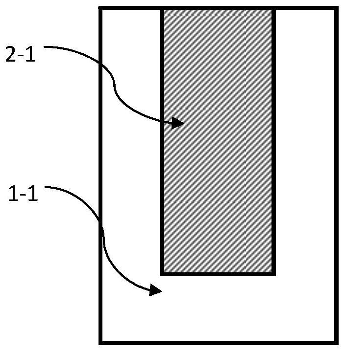
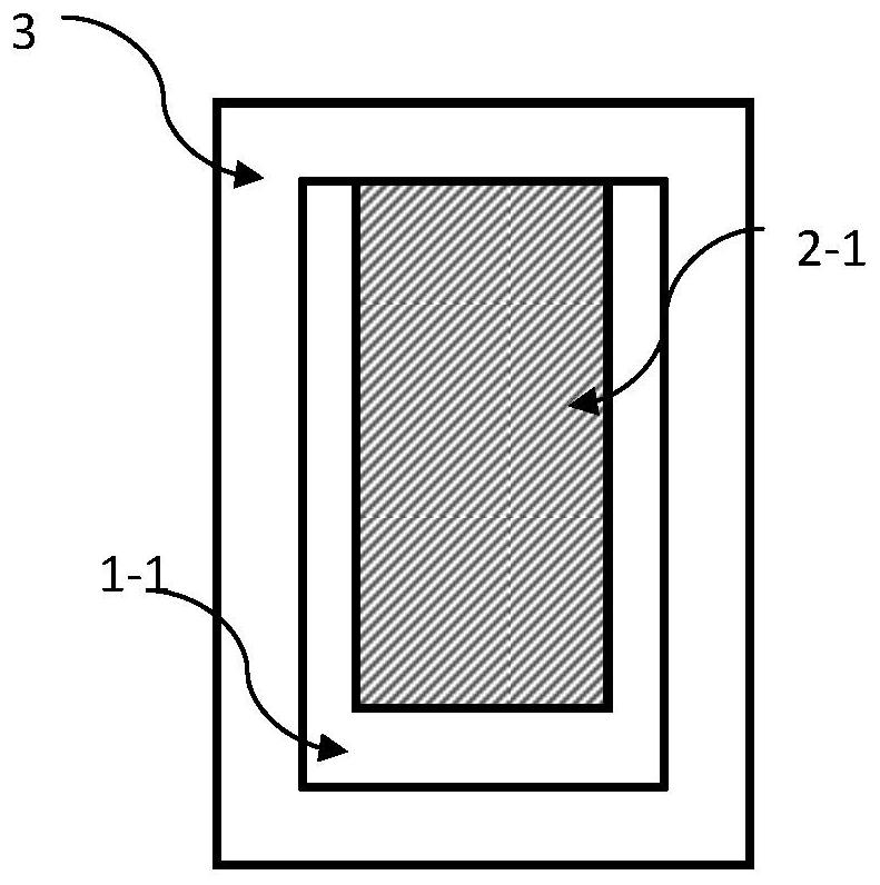
[0076] (1) On the lower substrate of the tape-cast glass ceramic body with a thickness of 10-12 μm, screen-print the first side electrode layer, the electrode is silver-palladium paste, and dry at 100 ° C for 20 minutes;

[0077] (2) On the basis of drying the electrode layer on the first side, print a rectangular cavity structure layer in the middle of the glass ceramic body, with a thickness of 28-32 μm, and dry it at 100° C. for 20 minutes;

[0078] (3) On the basis of drying the rectangular cavity structure layer in the middle of the glass ceramic body, print a pressure-sensitive material filling layer, the main component of which is ZnO, and dry it at 100°C for 20 minutes;

[0079] (4) Print the second side electrode layer on the basis of drying the pressure-sensitive material filling layer, the electrode is silver-palladium paste, and dry at 100°C for 20 minutes;

...

Embodiment 2

[0085] Take the overall dimension of a single product: (1.0±0.15)*(0.5±0.15)*(0.5±0.15)mm as an example;

[0086] (1) On the lower substrate of the glass-ceramic body with a thickness of 10-12 μm, screen-print the first side electrode layer, the electrode is pure palladium paste, and dry at 100°C for 20 minutes;

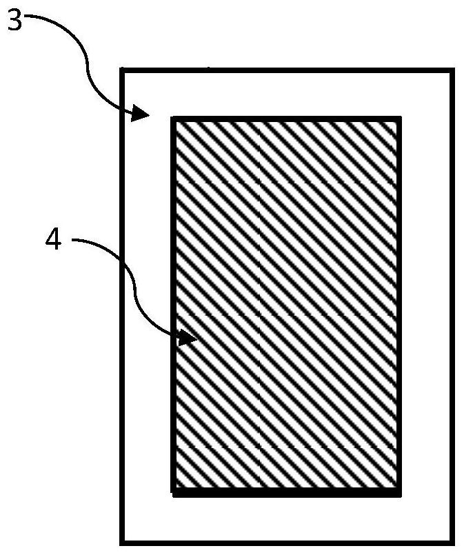
[0087] (2) On the basis of drying the electrode layer on the first side, print a rectangular cavity structure layer in the middle of the glass ceramic body, with a thickness of 38-42 μm, and dry it at 100° C. for 20 minutes;

[0088] (3) On the basis of drying the rectangular cavity structure layer in the middle of the glass ceramic body, print a pressure-sensitive material filling layer, the main component of which is ZnO, and dry it at 100°C for 20 minutes;

[0089] (4) On this basis, repeat steps (2) and (3) for 5 times, so that the thickness of the intermediate layer is 190-210 μm;

[0090] (5) Print the second side electrode layer on the basis of drying the pre...


PUM

PropertyMeasurementUnit
thicknessaaaaaaaaaa
thicknessaaaaaaaaaa
thicknessaaaaaaaaaa

Abstract

A laminated chip varistor and a manufacturing method thereof, the method comprising the following steps: S1, forming a first side electrode layer on a lower substrate of a glass ceramic material; S2, forming a glass electrode layer on the first side electrode layer A hollow cavity structure layer of ceramic material, the hollow cavity structure layer has a continuous outer peripheral wall, and an intermediate cavity is formed by the outer peripheral wall; S3, filling the intermediate cavity with a pressure-sensitive material layer; S4, forming a second side electrode layer on the hollow cavity structure layer and the pressure-sensitive material filling layer; S5, forming an upper substrate of glass-ceramic material on the last formed electrode layer; S6, after processing to Finished product preparation. The multilayer chip varistor of the present invention not only does not need any complicated surface treatment process, but also can effectively improve the surface insulation properties of the product, and is beneficial to improve the current flow, energy or varistor voltage of the product.

Description

technical field [0001] The invention relates to a laminated chip piezoresistor and a manufacturing method thereof. Background technique [0002] In the molding and manufacturing process of traditional multilayer chip varistors, since the pressure-sensitive materials are mainly semiconductor materials, such as zinc oxide, etc., surface treatment is required, usually by coating a layer of insulating resin, glass or other inorganic materials with good insulation properties. Salt to improve the problem of creeping plating in the electroplating process, but the conventional coating process cannot ensure that the surface layer is 100% dense, so the problem of plating creeping cannot be eliminated; at the same time, pressure-sensitive materials such as zinc oxide have poor compactness and are easy to absorb moisture. Therefore, if the surface coating layer of the product is not dense, it is easy to cause failure problems such as surface short circuit in the hot and humid environmen...

Claims


Application Information

Patent Timeline
Patent Type & Authority Patents(China)
IPC IPC(8): H01C17/00H01C17/065H01C17/28H01C7/112H01C7/115H01C7/118H01C1/142
CPCH01C1/142H01C7/112H01C7/115H01C7/118H01C17/00H01C17/065H01C17/28
Inventor 刘旭姚斌王清华
Owner SHENZHEN SUNLORD ELECTRONICS
Why Eureka
Try Eureka