Preparation method of power packaging module, power packaging module and storage medium
A technology for encapsulating modules and power, which is applied in semiconductor/solid-state device manufacturing, electrical components, circuits, etc., and can solve the problems of delamination of the package, poor bonding force between the lead frame and epoxy resin, reduction of moisture and heat resistance of power modules, and reliability. performance and service life
- Summary
- Abstract
- Description
- Claims
- Application Information
AI Technical Summary
Problems solved by technology
Method used
Image
Examples
Embodiment 1
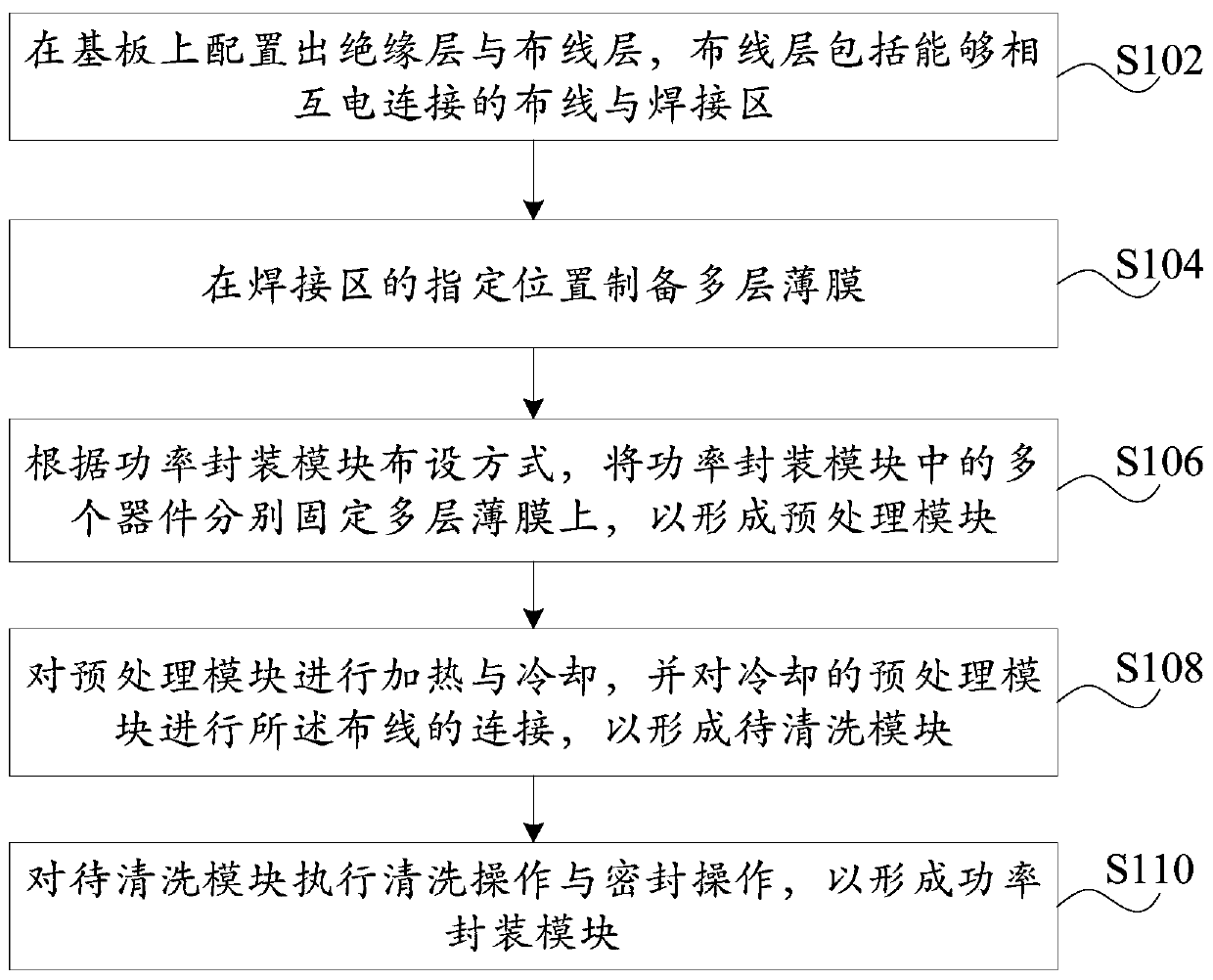
[0042] Such as figure 1 As shown, the preparation method of a power package module according to an embodiment of the present invention includes:
[0043] In step S102, an insulating layer and a wiring layer are arranged on the substrate, and the wiring layer includes wiring and soldering areas capable of being electrically connected to each other.
[0044] Step S104, preparing a multi-layer film at a designated position of the welding area.
[0045] Wherein, the introduction of solder and soldering flux in the solder layer is beneficial to be reduced by arranging multi-layer thin films.
[0046] In step S106, according to the layout of the power packaging module, a plurality of devices in the power packaging module are respectively fixed on multi-layer films to form a pretreatment module.
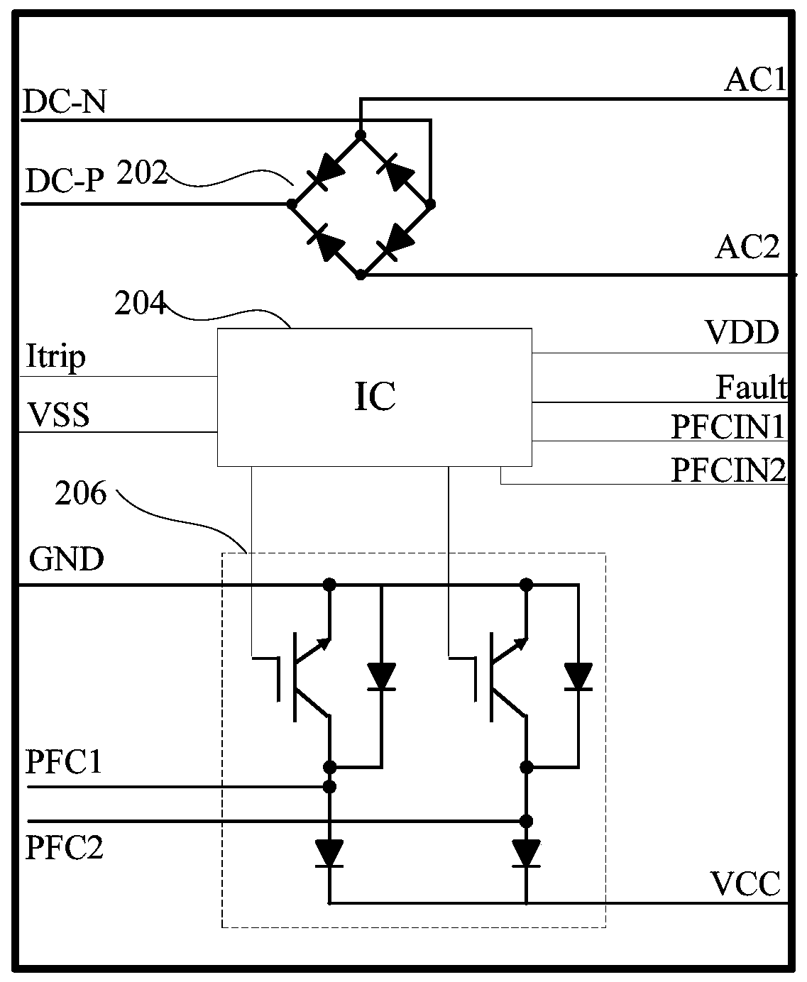
[0047] Specifically, such as figure 2 As shown, as a layout method of the power package module, it specifically includes: the first rectification output pin DC-N, the second rectificati...
Embodiment 2
[0086] The power package module according to an embodiment of the present invention is prepared by the above preparation method.
[0087] The power packaging module may specifically include a substrate; an insulating layer covering the substrate; a wiring layer arranged on the insulating layer; multiple devices and the wiring layer can configure a power drive circuit in the power packaging module; the multiple devices include: a rectifier, It is used to convert the input AC signal into a DC signal; the power factor correction module is arranged on the substrate and can be electrically connected to the output terminal of the rectifier to receive the DC signal; the control chip is electrically connected to the power factor correction module for The control signal is output to the power factor correction module, and the power factor correction module performs a power factor correction operation on the DC signal according to the control signal.
[0088] In this embodiment, a method ...
PUM
 Abstract
Description
Claims
Application Information


