
Quantum dot display panel brightness enhancement film and lens array

一种显示面板、透镜阵列的技术,应用在仪器、电气元件、电路等方向,能够解决影响使用者观看体验、降低量子点显示面板显示对比度等问题,达到增强广视角显示效果、减少激发的效果

Active Publication Date: 2020-03-27
SHENZHEN CHINA STAR OPTOELECTRONICS SEMICON DISPLAY TECH CO LTD
View PDF3 Cites 7 Cited by
  • Summary
  • Abstract
  • Description
  • Claims
  • Application Information

AI Technical Summary

Problems solved by technology

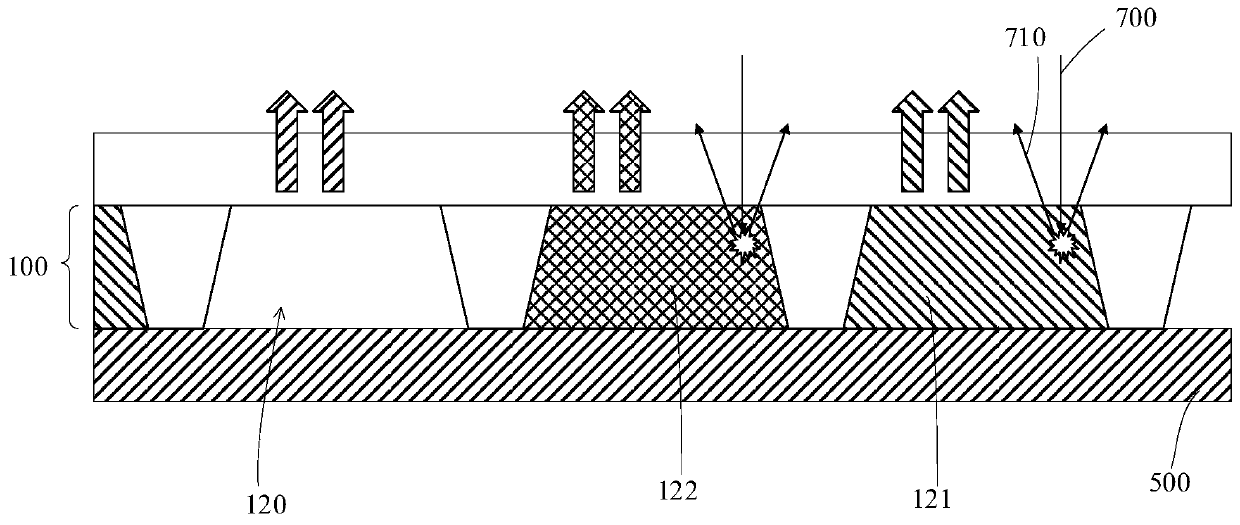
[0009] Therefore, even if the quantum dot display panel is displayed in a dark state, the ambient light excites the red quantum dots 121 and the green quantum dots 122 to emit light, which reduces the display contrast of the quantum dot display panel and affects the user's viewing experience

Method used


Image

  • Quantum dot display panel brightness enhancement film and lens array
  • Quantum dot display panel brightness enhancement film and lens array
  • Quantum dot display panel brightness enhancement film and lens array

Examples


no. 1 example

[0029] Figure 2 ~ Figure 6 It is a structural schematic diagram of the manufacturing process of the first embodiment of the quantum dot display panel of the present invention.

[0030] First, if figure 2 As shown, a resin 211a is coated on the substrate 400, and the resin 211a can also be replaced by other organic materials.

[0031] Second, if image 3 As shown, will figure 2 The resin 211a in the embossing method forms a lens array 210 composed of a plurality of convex lenses 211 .

[0032] Third, if Figure 4 As shown, a lens flat layer 212 is formed on the lens array 210 , and the side of the lens flat layer 212 opposite to the lens array 210 is a flat surface, which is convenient for subsequent processes.

[0033] Fourth, if Figure 5 As shown, the pixel layer 100 is disposed on the lens planar layer 212 . In the pixel layer 100, a plurality of barrier walls 110 are formed through photolithography or inkjet printing process, the position of each barrier wall 110...

no. 2 example

[0045] Figure 9 ~ Figure 10 It is a structural schematic diagram of the manufacturing process of the second embodiment of the quantum dot display panel of the present invention.

[0046] First, if Figure 9 As shown, on the substrate 400, a plurality of barrier walls 110 are formed through a photolithography or inkjet printing process, and a plurality of sub-pixels 120 can be defined between the plurality of barrier walls 110, and each of the three sub-pixels 120 The two sub-pixels 120 are filled with photoluminescent red quantum dots 121 and green quantum dots 122 through photolithography or inkjet printing process.

[0047] A blue backlight 500 is pasted on the side of the plurality of sub-pixels 120 opposite to the substrate 400, and the blue backlight 500 is a blue organic light-emitting diode (blue organic light-emitting diode, blue OLED) light source Or a blue micro light-emitting diode (blue micro light-emitting diode, blue micro LED) light source. The light from th...


PUM

PropertyMeasurementUnit
diameteraaaaaaaaaa
diameteraaaaaaaaaa
quantum yieldaaaaaaaaaa

Abstract

The invention provides a quantum dot display panel. The quantum dot display panel comprises a pixel layer, a lens layer and a brightness enhancement film, wherein the pixel layer comprises a pluralityof retaining walls and a plurality of sub-pixels defined among the retaining walls, and two sub-pixels of every three sub-pixels are filled with red quantum dots and green quantum dots; the lens layer is arranged on the pixel layer and comprises a lens array composed of a plurality of convex lenses, and the focus of each lens is located in the corresponding retaining wall; the brightness enhancement film is arranged on the lens layer and comprises a prism array composed of a plurality of prisms facing the pixel layer. When the ambient light enters the quantum dot display panel, the ambient light is converged and collimated through the brightness enhancement film; and then the ambient light is converged to a plurality of retaining walls with light absorption characteristics by the lens array. The lens array maintains the contrast of the quantum dot display panel; the brightness enhancement film enhances the wide-viewing-angle display effect of the quantum dot display panel.

Description

technical field [0001] The invention relates to the technical field of quantum dot display panels, in particular to a brightness enhancement film and a lens array for a quantum dot display panel. Background technique [0002] Quantum dots (quantum dot, QD) are tiny semiconductor particles at the nanometer scale, whose optical and electronic properties are different from larger general particles due to quantum mechanics. When the quantum dots receive external light, the electrons in the quantum dots will be excited, and the electrons will jump from the valence band to the conduction band. When the excited electrons return to the valence band again, they will release their energy with light emission. This is the so-called photo-emissive quantum dot. In addition, the quantum dots will also receive the energy provided by the electric field to generate light, which is the so-called electro-emissive quantum dots. [0003] The size of quantum dots affects their light-emitting pro...

Claims


Application Information

Patent Timeline
Patent Type & Authority Applications(China)
IPC IPC(8): G02F1/1335H01L27/32H01L51/52
CPCG02F1/133526G02F1/133504G02F1/133507H10K59/35H10K59/122H10K59/879H01L25/0753H01L33/504H01L33/58H01L2933/0041H01L25/167H10K59/38H10K2102/331H01L27/156H01L33/005H01L33/04H01L2933/0058
Inventor 潘甦
Owner SHENZHEN CHINA STAR OPTOELECTRONICS SEMICON DISPLAY TECH CO LTD
Learn More