Semiconductor interconnection structure and preparation method thereof

An interconnect structure and semiconductor technology, applied in semiconductor/solid-state device manufacturing, semiconductor devices, semiconductor/solid-state device components, etc., can solve problems such as large contact resistance conductive plugs, increased conductive plug resistance, and affecting device electrical performance , to achieve the effect of increasing the contact surface, reducing the contact resistance and reducing the resistance

Inactive Publication Date: 2020-03-27
SIEN QINGDAO INTEGRATED CIRCUITS CO LTD
View PDF0 Cites 3 Cited by
  • Summary
  • Abstract
  • Description
  • Claims
  • Application Information

AI Technical Summary

Problems solved by technology

However, as the size of the conductive plug decreases, the contact area between the conductive plug and the underlying metal layer also decreases, which will inevitably increase the contact resistance between the two; Copper is filled in the through hole as the conductive plug, and the filling ability of copper is relatively poor. Air holes are formed in the conductive plug, which will further increase the resistance of the conductive plug
Too much contact resistance between the conductive plug and the metal layer and too much resistance of the conductive plug itself will affect the electrical performance of the device

Method used


Image

  • Semiconductor interconnection structure and preparation method thereof
  • Semiconductor interconnection structure and preparation method thereof
  • Semiconductor interconnection structure and preparation method thereof

Examples


Embodiment 1

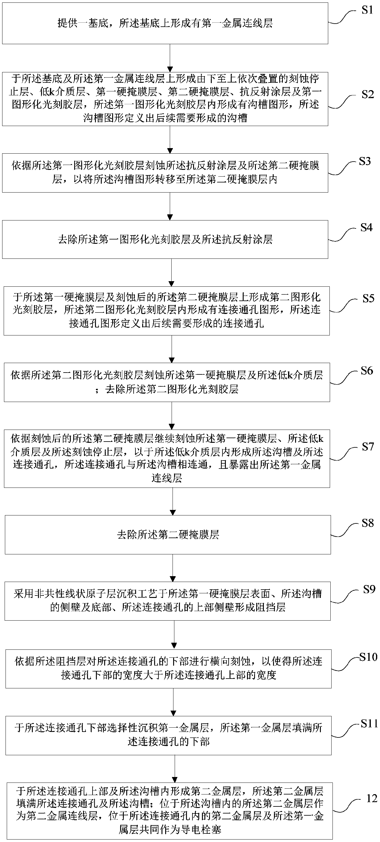
[0071] see figure 1 , the present invention provides a method for preparing a semiconductor interconnection structure, the method for preparing a semiconductor interconnection structure includes the following steps:

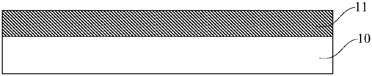
[0072] 1) providing a base, on which a first metal wiring layer is formed;

[0073] 2) Forming an etch stop layer, a low-k dielectric layer, a first hard mask layer, a second hard mask layer, an anti-reflection layer stacked sequentially from bottom to top on the base and the first metal wiring layer A coating layer and a first patterned photoresist layer, wherein groove patterns are formed in the first patterned photoresist layer, and the groove patterns define grooves to be formed subsequently;

[0074] 3) etching the anti-reflection coating and the second hard mask layer according to the first patterned photoresist layer, so as to transfer the groove pattern into the second hard mask layer;

[0075] 4) removing the first patterned photoresist layer and the a...

Embodiment 2

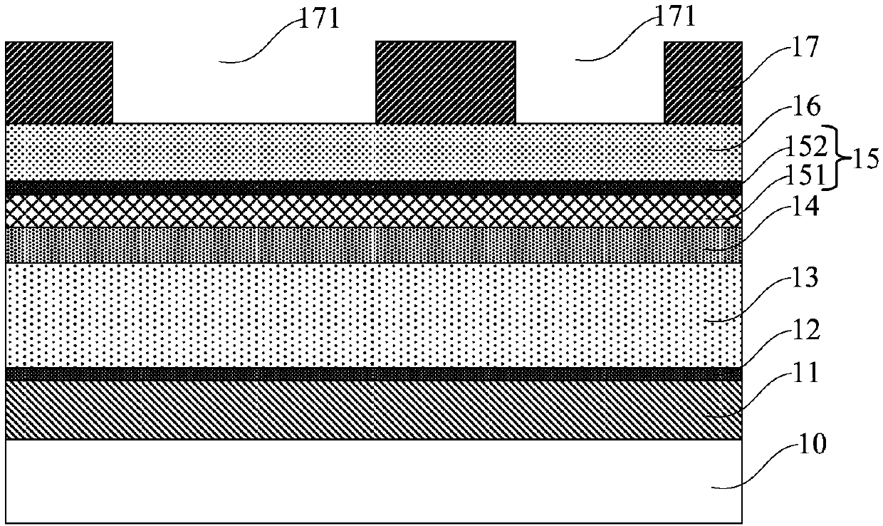
[0125] Please combine Figure 1 to Figure 15 refer to Figure 16 , the present invention also provides a semiconductor interconnection structure, which can be prepared by using but not limited to the preparation method described in Embodiment 1. The semiconductor interconnection structure includes:

[0126] A first metal wiring layer 11; the first metal wiring layer 11 may be formed on a substrate 10;

[0127] an etch stop layer 12, the etch stop layer 12 is located on the first metal wiring layer 11;

[0128] a low-k dielectric layer 13, the low-k dielectric layer 13 is located on the etching stop layer 12;

[0129] A conductive plug 22, the conductive plug 22 is located in the low-k dielectric layer 13 and the etching stop layer 13, the conductive plug 22 includes a first metal layer 221 and a second metal layer 222; the first metal layer The bottom of the layer 221 is in contact with the first metal wiring layer 11, and the width of the first metal layer 221 is greater t...


PUM

PropertyMeasurementUnit
thicknessaaaaaaaaaa

Abstract

The invention provides a semiconductor interconnection structure and a preparation method thereof, and the method comprises the steps: 1), providing a substrate which is provided with a first metal connecting line layer; 2) forming an etching stop layer, a low-k dielectric layer, a first hard mask layer, a second hard mask layer, an anti-reflection coating and a first graphical photoresist layer on the substrate and the first metal connecting line layer; 3) etching the anti-reflection coating and the second hard mask layer; 4) removing the first graphical photoresist layer and the anti-reflection coating; 5) forming a second graphical photoresist layer; 6) etching the first hard mask layer and the low-k dielectric layer; 7) continuously etching the first hard mask layer, the low-k dielectric layer and the etching stop layer to form a groove and a connecting through hole; 8) removing a second hard mask layer; 9) forming a barrier layer; 10) transversely etching the lower portion of theconnecting through hole; (11) selectively depositing a first metal layer on the lower portion of the connecting through hole, and (12) forming a second metal layer. The preparation method can reduce contact resistance between the conductive plug and the first metal connecting line layer.

Description

technical field [0001] The invention relates to the technical field of semiconductors, in particular to a semiconductor interconnection structure and a preparation method thereof. Background technique [0002] With the shrinking of process nodes, the minimum spacing between metal layers becomes smaller and smaller, and the size of conductive plugs between metal layers becomes smaller and smaller. However, as the size of the conductive plug decreases, the contact area between the conductive plug and the underlying metal layer also decreases, which will inevitably increase the contact resistance between the two; Copper is filled in the through hole as the conductive plug, and the filling ability of copper is relatively poor. Air holes are formed in the conductive plug, which will further increase the resistance of the conductive plug. Too much contact resistance between the conductive plug and the metal layer and too much resistance of the conductive plug itself will affect ...

Claims


Application Information

Patent Timeline
Patent Type & Authority Applications(China)
IPC IPC(8): H01L21/768H01L23/528
CPCH01L21/76879H01L23/5283H01L2221/1068
Inventor 平延磊杨瑞鹏肖德元
Owner SIEN QINGDAO INTEGRATED CIRCUITS CO LTD
Why Eureka
Try Eureka