Cutting method for improving utilization rate of monocrystalline silicon rod

A cutting method and monocrystalline silicon ingot technology, applied in fine working devices, stone processing equipment, manufacturing tools, etc., can solve the problems of increasing the carbon footprint consumption of monocrystalline silicon wafers, increasing production costs, and consuming a large amount of electric energy, etc., to achieve Improve effective utilization, save processing costs, and save costs

Inactive Publication Date: 2020-04-10
江苏美科太阳能科技股份有限公司 +1
View PDF9 Cites 8 Cited by
  • Summary
  • Abstract
  • Description
  • Claims
  • Application Information

AI Technical Summary

Problems solved by technology

[0004] The drawing of a single wafer rod requires a large amount of electric energy, inert gas, thermal field composed of high-purity graphite materials, furnace equipment, etc., resulting in high non-silicon cost of the round rod (or single crystal silicon wafer), accounting for the current single cry

Method used


Image

  • Cutting method for improving utilization rate of monocrystalline silicon rod
  • Cutting method for improving utilization rate of monocrystalline silicon rod

Examples


Embodiment 1

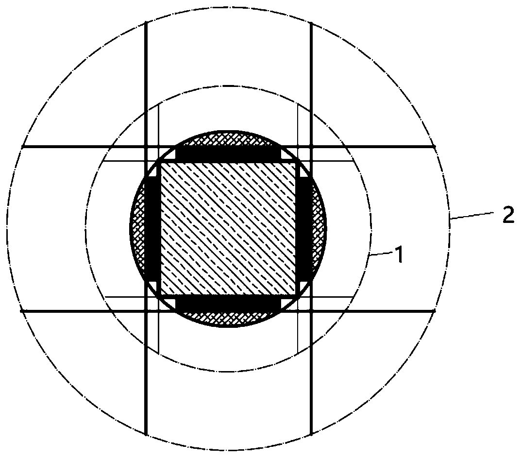
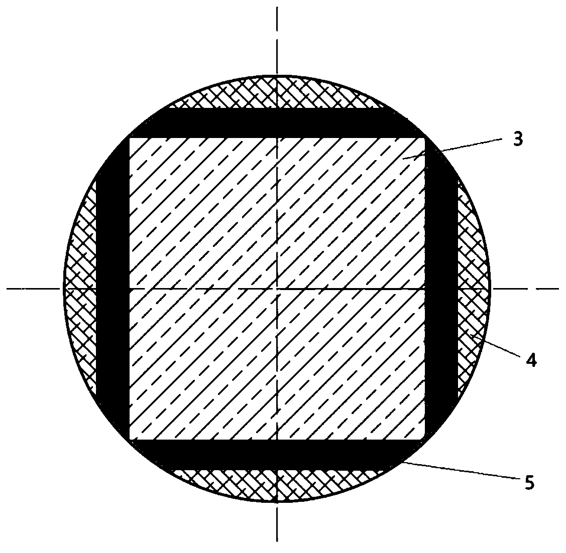
[0021] 1. Cut the truncated single crystal round bar with a length of 650mm and a diameter of 300mm, using the inner network cable 1 and the outer network cable 2 to cut a single crystal square bar 3 with a side length of 210mm, and produce four pieces of 20mm thick and 650mm long A single-crystal slab 5 with an arc and four arch-shaped single-crystal edges 4 with a thickness of about 25 mm.

[0022] 2. Bond a certain amount of monocrystalline slabs together with hydrosol, and use a diamond wire cutting machine to cut the two sides of the monocrystalline slabs in arcs to produce a rectangular parallelepiped silicon block with a side length of 158mm and a thickness of 20mm.

[0023] 3. Bond the cuboid silicon blocks together with water sol, cut them into squares with a size of 158mm, and use water sol to bond them to form a composite "square rod" with a length of 640-650mm.

[0024] 4. Put the square bar produced in step (3) on the surface after polishing, and slice it with a d...

Embodiment 2

[0027] 1. Cut the truncated single crystal round bar with a length of 650mm and a diameter of 300mm, using the inner network cable 1 and the outer network cable 2 to cut a single crystal square bar 3 with a side length of 210mm, and produce four pieces of 20mm thick and 650mm long A single-crystal slab 5 with an arc and four arch-shaped single-crystal edges 4 with a thickness of about 25 mm.

[0028] 2. Bond a certain amount of monocrystalline slabs together with hydrosol, and use a diamond wire cutting machine to cut the two sides of the monocrystalline slabs in arcs to produce a rectangular parallelepiped silicon block with a side length of 158mm and a thickness of 20mm.

[0029] 3. Cut the rectangular parallelepiped silicon block into 158mm in length and 20mm in thickness, and use it as seedlings for casting single crystal silicon, and lay it on the bottom of the crucible to induce the growth of quasi-single crystal crystals with a single crystal orientation.


PUM

PropertyMeasurementUnit
Diameteraaaaaaaaaa

Abstract

The invention discloses a cutting method for improving the utilization rate of a monocrystalline silicon rod. The method comprises the steps of: adding a set of cutting wire net extending outwards for20mm besides the original cutting of a 210mm extraction wire net; after cutting, generating a square rod with the side length of 210 mm, four single crystal plate blanks with the thickness of 20 mm and arc sides and four arched single crystal edge skins with the thickness of about 25 mm; and bonding the plurality of single crystal plate blanks by using hydrosol, cutting edges by using a diamond wire cutting machine, and correcting the single crystal plate blanks into rectangular single crystal plate blanks with the thickness of 20mm, the side length of 158mm and the length equal to that of around rod. According to the cutting method, the volume ratio of available partial crystals after cutting of the monocrystalline silicon rod can be increased, the effective utilization rate of the monocrystalline silicon rod is increased, and the production cost is greatly saved.

Description

technical field [0001] The invention relates to a method for improving the utilization rate of monocrystalline silicon rods, and belongs to the technical field of photovoltaic grade monocrystalline silicon production. Background technique [0002] With the large-scale application of diamond wire slicing and the application of high-efficiency cell technologies such as PERC and HIT, monocrystalline silicon wafers have gradually become the main substrate material for photovoltaic cells due to their advantages such as fewer defects, high carrier lifetime, and stable quality. [0003] The monocrystalline silicon wafers currently used in photovoltaic cells are cut into squares by pulling a single wafer rod and then cut with a diamond wire. The edge material produced by cutting the round bar into squares is reused as a recycled material after cleaning. The crystal (square bar or quasi-square bar) used to cut silicon wafers accounts for only 60%-70%, and 30-40%. Single crystal mate...

Claims


Application Information

Patent Timeline
IPC IPC(8): B28D5/00B28D5/04
CPCB28D5/0058B28D5/045
Inventor 张志强王艺澄周炎姚亮
Owner 江苏美科太阳能科技股份有限公司
Why Eureka
Try Eureka