
Method for improving overflow plating and adhesive force performance of chemical plating layer in LDS process

An adhesion and coating technology, applied in electrical components, printed circuit manufacturing, conductive pattern formation, etc., can solve problems such as failure to pass the 100-grid test, insufficient adhesion of the chemical plating layer, short circuit of adjacent lines, etc., to improve the overflow plating. and adhesion performance, the effect of reducing the risk of overplating

Inactive Publication Date: 2020-04-10
SHANGHAI AMPHENOL AIRWAVE COMM ELECTRONICS CO LTD
View PDF4 Cites 0 Cited by
  • Summary
  • Abstract
  • Description
  • Claims
  • Application Information

AI Technical Summary

Problems solved by technology

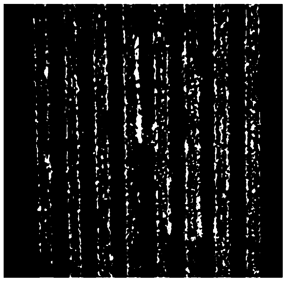
However, in order to increase the strength, the current plastic materials usually contain glass fiber components. When the laser is irradiated with high intensity, the glass fiber often protrudes, and the glass fiber is very easy to be plated, especially for small-pitch circuits. The laser activates the plastic material, which is easy to cause a short circuit in the adjacent circuit, such as figure 2 As shown, the chemical plating layer of adjacent lines is connected; in order to avoid the situation of overflow plating, laser activation of plastic materials is performed with low-power laser, which will cause the metal particles in the LDS substrate to not be fully activated, which will lead to poor adhesion of the chemical plating layer. Not enough, the 100 grid test cannot pass

Method used


Image

  • Method for improving overflow plating and adhesive force performance of chemical plating layer in LDS process
  • Method for improving overflow plating and adhesive force performance of chemical plating layer in LDS process
  • Method for improving overflow plating and adhesive force performance of chemical plating layer in LDS process

Examples


Embodiment Construction

[0021] A method for improving the overflow plating and adhesion performance of the electroless plating layer in the LDS process proposed by the present invention will be further described in detail below in conjunction with the accompanying drawings and specific examples. Advantages and features of the present invention will be apparent from the following description and claims.

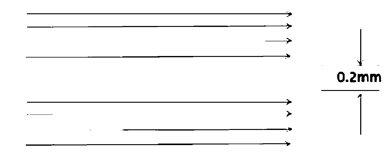
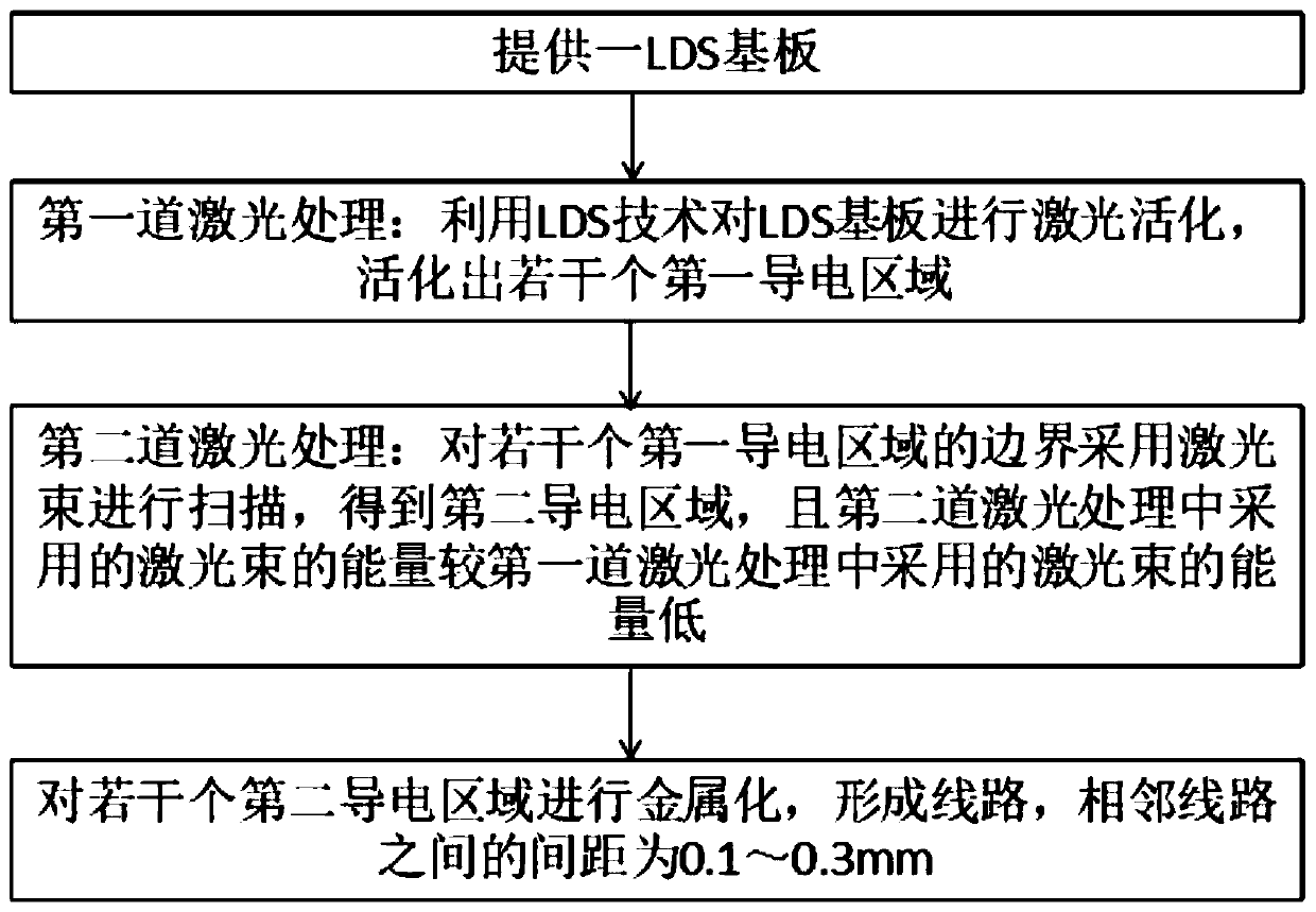
[0022] see image 3 , Figure 4 Shown, the present invention provides a kind of method that improves chemical coating overflow plating and adhesion performance in LDS technology, comprises the steps:

[0023] Provide an LDS substrate, the LDS substrate of the present embodiment selects the LCP material containing glass fiber of Celanese company, the intensity of this kind substrate is better;

[0024] The first laser treatment: use LDS technology to perform laser activation on the LDS substrate to activate several first conductive regions. In the first laser treatment step, see Figure 4 As shown ...


PUM


Abstract

The invention provides a method for improving overflow plating and adhesion performance of a chemical plating layer in an LDS process. The method comprises the following steps of: performing laser activation on a substrate by using an LDS technology to activate a plurality of first conductive regions; scanning the boundaries of the plurality of first conductive regions by adopting laser beams to obtain second conductive regions, and the energy of the laser beams adopted in the second laser processing being lower than that of the laser beams adopted in the first laser processing; and metallizing the plurality of second conductive regions to form circuits, the distance between the adjacent circuits being 0.1-0.3 mm. According to the invention, a laser treatment process is added on the basisof the existing LDS process. The substrate is firstly subjected to laser activation by adopting the laser with higher power, and then the boundary of the activation area is subjected to laser activation by adopting the laser with lower power, so that when the method is used for processing the circuit board with the small-spacing circuit, the risk of overflow plating of the chemical plating layer can be reduced, and the adhesive force of the chemical plating layer can be ensured to pass a hundred-grid test.

Description

technical field [0001] The invention belongs to the technical field of LDS, in particular to a method for improving the overflow plating and adhesion performance of the electroless coating in the LDS process. Background technique [0002] Laser direct structuring (LDS) technology uses a computer to control the movement of the laser according to the trajectory of the conductive pattern, projects the laser onto the plastic device, and activates the circuit pattern within a few seconds. [0003] The current conventional LDS technical process is as follows: see figure 1 As shown, the LDS substrate is first activated by laser, the activation path is shown by the arrow in the figure, and then metallization is performed on the activated area to form a circuit. However, in order to increase the strength, the current plastic materials usually contain glass fiber components. When the laser is irradiated with high intensity, the glass fiber often protrudes, and the glass fiber is very...

Claims


Application Information

Patent Timeline
Patent Type & Authority Applications(China)
IPC IPC(8): H05K3/10
CPCH05K3/105H05K2203/107
Inventor 马承文张文宇孔维贞胡宗亮张东胜
Owner SHANGHAI AMPHENOL AIRWAVE COMM ELECTRONICS CO LTD
Learn More