A near-ultraviolet LED using MOCVD technology and its preparation method

A near-ultraviolet, high-tech technology, applied in semiconductor devices, electrical components, circuits, etc., can solve the problems of electronic current leakage, low quantum efficiency and luminous efficiency of devices, and leakage, so as to improve crystal quality, improve polarization effect, reduce The effect of stress

Active Publication Date: 2021-01-19
GUANGDONG INST OF SEMICON IND TECH
View PDF6 Cites 0 Cited by
  • Summary
  • Abstract
  • Description
  • Claims
  • Application Information

AI Technical Summary

Problems solved by technology

A key factor that limits the luminous efficiency of GaN-based LEDs is the mismatch of electron-hole injection under high current conditions, resulting in electron current leakage, that is, some electrons cannot fully recombine in the light-emitting active region and emit light from the active region. Leakage into the p-type region, resulting in lower quantum efficiency and luminous efficiency of the device

Method used


Image

  • A near-ultraviolet LED using MOCVD technology and its preparation method
  • A near-ultraviolet LED using MOCVD technology and its preparation method
  • A near-ultraviolet LED using MOCVD technology and its preparation method

Examples


no. 1 example

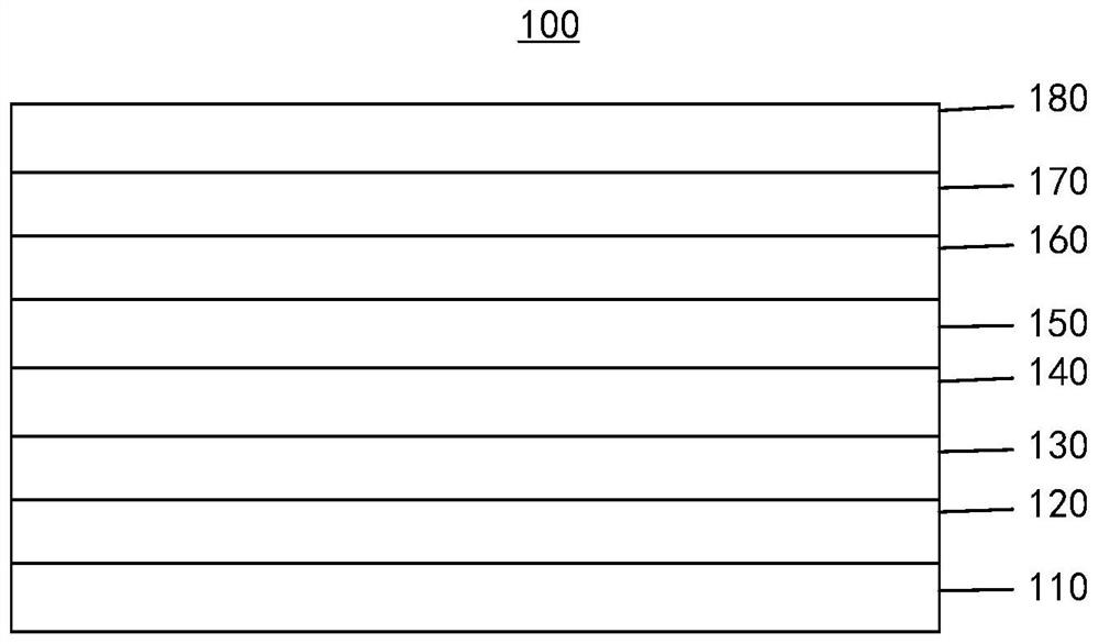
[0042] see figure 1 , this embodiment provides a near-ultraviolet LED 100 using MOCVD technology. The near-ultraviolet LED 100 includes a substrate 110 and a buffer layer 120, a high-temperature layer 130, and an n-type Al layer grown sequentially on the substrate 110. m Ga 1-m N layer 140, light emitting active region 150, p-type electron blocking layer 160, p-type Al n Ga 1-n N layer 170 and contact layer 180, wherein the material of the light emitting active region 150 includes In x Ga 1-x N and Al y Ga 1-y N, the material of the p-type electron blocking layer 160 includes Al y1 In x1 Ga 1-y1- x1 N, 0.001≤x

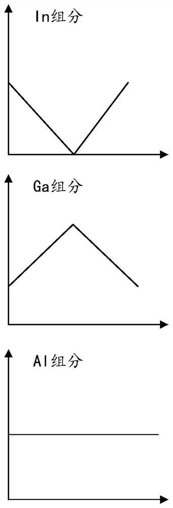
[0043] see figure 2 , along the growth direction of the p-type electron blocking layer 160, the Al composition value y1 remains unchanged, the In composition value x1 first decreases and then increases, and the Ga composition value 1-y1-x1 first increases and then decreases. Preferably, the In composition value x1 present...

no. 2 example

[0050] This embodiment provides a near-ultraviolet LED 100 using MOCVD technology, which is similar to the structure in the first embodiment, except that the lowest value x1 of the In composition in the p-type electron blocking layer 160 is greater than zero.

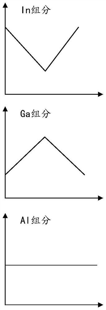
[0051] see image 3 , along the growth direction of the p-type electron blocking layer 160, the Al composition value y1 remains unchanged, the In composition value x1 presents a V-shaped gradual change, and the Ga composition value 1-y1-x1 presents an inverted V-shaped gradual change. Furthermore, the Ga composition value 1-y1-x1 is the highest at the position where the In composition value x1 is the lowest.

[0052] Wherein, the In composition value x1 is greater than zero at the lowest point, that is to say, the p-type electron blocking layer 160 is AlInGaN along the growth direction.

[0053] In addition, in the p-type electron blocking layer 160 , in the direction from the edge to the middle, the Mg doping concentr...

no. 3 example

[0058] see Figure 4 , this embodiment provides a method for preparing a near-ultraviolet LED 100 using MOCVD technology, which can be used to prepare the near-ultraviolet LED 100 in the first embodiment or the second embodiment. The preparation method of the near-ultraviolet LED 100 is mainly based on the MOCVD epitaxial growth technology, and specifically includes the following steps:

[0059] S1: see Figure 5 , on the substrate 110, the buffer layer 120, the high temperature layer 130, the n-type Al m Ga 1-m N layer 140 and light emitting active region 150 .

[0060] First, grow a GaN buffer layer 120 with a thickness of 1 micron to 3 microns on the PSS substrate 110 in a hydrogen atmosphere at a temperature of 800° C. to 1000° C. in the reaction chamber of the MOCVD epitaxial equipment.

[0061] Next, the temperature is increased to 1000° C.˜1150° C. to grow the high-temperature layer 130 with a thickness of 1 μm˜4 μm; the growth pressure is controlled between 100 mba...


PUM

PropertyMeasurementUnit
thicknessaaaaaaaaaa
thicknessaaaaaaaaaa

Abstract

The invention provides a near ultraviolet LED adopting an MOCVD technology and a preparation method thereof, and relates to the technical field of semiconductors. The near ultraviolet LED comprises asubstrate, and a buffer layer, a high-temperature layer, an n-type AlmGa1-mN layer, a light-emitting active region, a p-type electron blocking layer, a p-type AlnGa1-nN layer and a contact layer whichare sequentially grown on the substrate, wherein the material of the light-emitting active region comprises In < x > Ga < 1-x > N and Al < y > Ga < 1-y > N, the material of the p-type electron blocking layer comprises Al < y 1> In < x 1> Ga < 1-y1-x1 > N, 0.001<=x<y<=1, and y, m and n are all less than y1. The near ultraviolet LED can effectively improve the electron limiting effect and the holeinjection efficiency, so that the quantum efficiency and the light emitting efficiency of the device are improved.

Description

technical field [0001] The invention relates to the technical field of semiconductors, in particular to a near-ultraviolet LED using MOCVD technology and a preparation method thereof. Background technique [0002] In recent years, LED has experienced an unusually rapid development. According to reports, the theoretical maximum efficiency of white LEDs is as high as 400lm / W, far exceeding traditional lighting fixtures (incandescent lamps, fluorescent lamps, etc.). Although GaN-based LEDs have achieved good development, there is still a lot of room for development compared to their theoretical maximum efficiency. A key factor limiting the luminous efficiency of GaN-based LEDs is the mismatch of electron-hole injection under high current conditions, resulting in electron current leakage, that is, some electrons cannot fully recombine in the light-emitting active region and emit light from the active region. Leakage to the p-type region, resulting in low quantum efficiency and...

Claims


Application Information

Patent Timeline
Patent Type & Authority Patents(China)
IPC IPC(8): H01L33/14H01L33/12H01L33/32H01L33/02H01L33/00
CPCH01L33/0075H01L33/025H01L33/12H01L33/14H01L33/32H01L33/325
Inventor 贺龙飞赵维张康何晨光吴华龙廖乾光陈志涛
Owner GUANGDONG INST OF SEMICON IND TECH
Why Eureka
Try Eureka