Semiconductor structure and forming method thereof

A semiconductor and dummy gate technology, applied in the field of semiconductor structures and their formation, can solve problems such as poor performance of semiconductor structures and occupy space, and achieve the effects of solving the problem of etching residues, saving lateral space, and large process space

Pending Publication Date: 2020-04-21
SEMICON MFG INT (SHANGHAI) CORP +1
View PDF8 Cites 0 Cited by
  • Summary
  • Abstract
  • Description
  • Claims
  • Application Information

AI Technical Summary

Problems solved by technology

[0004] In the FinFET device, a dummy gate structure covering part of the top wall and part of the sidewall of the fin is formed first, and the dummy gate structure occupies space for forming a metal gate structure in a subsequent process, but the performance of the formed semiconductor structure is not good

Method used


Image

  • Semiconductor structure and forming method thereof
  • Semiconductor structure and forming method thereof
  • Semiconductor structure and forming method thereof

Examples


Embodiment Construction

[0032] It can be seen from the background art that the devices formed so far still have the problem of poor performance. Combining with a method of forming a semiconductor structure, the reason for the poor performance of the device is analyzed.

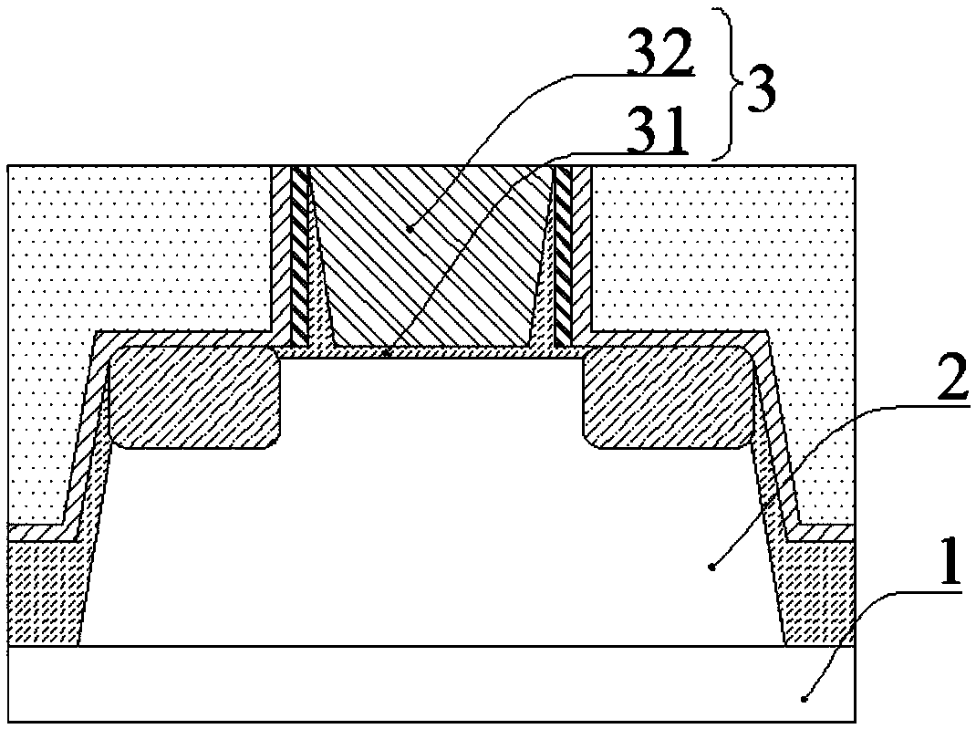
[0033] Reference 1 shows a schematic structural diagram corresponding to a method for forming a semiconductor structure.

[0034] refer to figure 1 , providing a base, the base includes a substrate 1, a discrete fin 2 protruding from the substrate 1, and a dummy gate structure 3 across the fin 2, the dummy gate structure 3 covers the fin Part of the top wall and part of the side wall of part 2.

[0035] The dummy gate structure 3 includes a dummy gate oxide layer 31 conformally covering part of the top wall and sidewall of the fin, and a dummy gate layer 32 located on the dummy gate oxide layer 31 . In the dummy gate layer 32, the length perpendicular to the sidewall direction of the dummy gate structure 3 is taken as the width, t...


PUM


Abstract

The invention relates to a semiconductor structure and a forming method thereof. The forming method comprises the steps of providing a base, wherein the base comprises a substrate and discrete fins arranged on the substrate in a protruding manner; forming a pseudo gate structure stretching across the fins, wherein the pseudo gate structure comprises a first pseudo gate layer and a second pseudo gate layer located on the first pseudo gate layer, the width of the first pseudo gate layer is gradually increased from bottom to top, and the side wall of the second pseudo gate layer is perpendicularto the top surface of the substrate; forming a source-drain doping layer in the fins on the two sides of the pseudo gate structure; forming a dielectric layer on the source-drain doping layer, whereinthe dielectric layer exposes the top of the pseudo gate structure; removing the pseudo gate structure, and forming an opening in the dielectric layer; and forming a metal gate structure filling the opening. The included angle between the side wall of the first pseudo gate layer and the top wall of the fin is less than 90 degrees, so that the process space for subsequently removing the first pseudo gate layer is large, and the first pseudo gate layer is not prone to being left. On the basis, the side wall of the second pseudo gate layer is perpendicular to the top surface of the substrate, sothat the transverse space of the top surface of the fin is saved, the further reduction of the device size is facilitated, and the performance of the semiconductor structure is optimized.

Description

technical field [0001] Embodiments of the present invention relate to the field of semiconductor manufacturing, and in particular to a semiconductor structure and a method for forming the same. Background technique [0002] In semiconductor manufacturing, with the development trend of ultra-large-scale integrated circuits, the feature size of integrated circuits continues to decrease. In order to adapt to smaller feature sizes, metal-oxide-semiconductor field-effect transistors (Metal-Oxide-Semiconductor Field-Effect Transistor , MOSFET) channel length has been shortened accordingly. However, as the channel length of the device is shortened, the distance between the source and the drain of the device is also shortened, so the control ability of the gate structure on the channel becomes worse, and the gate voltage pinches off the channel. The channel becomes more and more difficult, making subthreshold leakage (subthreshold leakage), the so-called short-channel effect (SCE: ...

Claims


Application Information

Patent Timeline
Patent Type & Authority Applications(China)
IPC IPC(8): H01L21/336H01L21/28H01L29/423H01L29/78
CPCH01L29/66795H01L29/785H01L29/4238H01L29/401
Inventor 王楠王颖倩
Owner SEMICON MFG INT (SHANGHAI) CORP
Why Eureka
Try Eureka