Method for opening terminal area of high-efficiency silicon-based micro display device

A technology of a microdisplay device and an opening method, which is applied in the manufacturing of semiconductor devices, electric solid-state devices, and semiconductor/solid-state devices, etc., can solve the problems of long process time, poor glue exposure and development, and poor bonding.

Pending Publication Date: 2021-06-08
ANHUI SEMICON INTEGRATED DISPLAY TECH CO LTD
View PDF6 Cites 0 Cited by
  • Summary
  • Abstract
  • Description
  • Claims
  • Application Information

AI Technical Summary

Problems solved by technology

[0003] At present, the process of opening the terminal area of ​​silicon-based micro OLED microdisplays is relatively complicated. The process is to first coat, expose, and develop to define the PAD position pattern, then perform dry etching to transfer the pattern to Die, and finally perform wet removal Photoresist: In the above process, poor glue exposure and development can easily cause PR abnormalities, affect graphic definition, poor dry etching, easy to produce residues

Method used


Image

  • Method for opening terminal area of high-efficiency silicon-based micro display device
  • Method for opening terminal area of high-efficiency silicon-based micro display device
  • Method for opening terminal area of high-efficiency silicon-based micro display device

Examples


Embodiment Construction

[0030] The specific implementation manner of the present invention will be described in further detail below by describing the embodiments with reference to the accompanying drawings.

[0031] Such as Figure 1 to Figure 6 As shown, the method for opening the terminal region of the high-efficiency silicon-based micro-display device comprises the following steps:

[0032] Step 1, PET tape bonding:

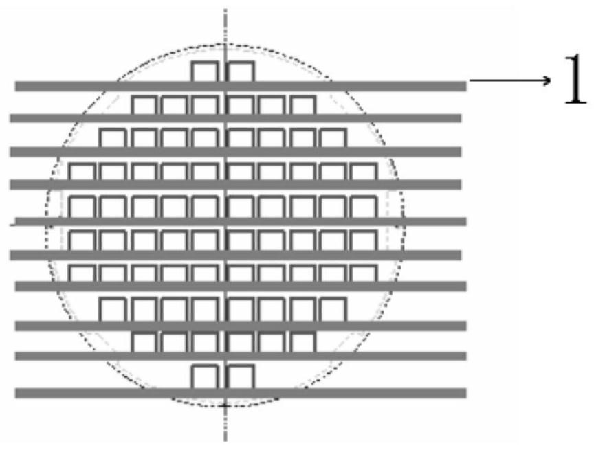
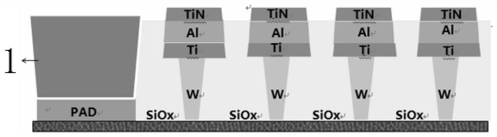
[0033] After completing the front-end process, stick PET tape on the PAD area;

[0034] Step 2. Encapsulation operation:

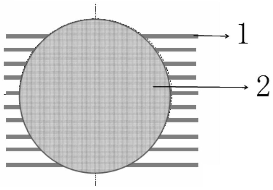
[0035] Perform OLED and film encapsulation operations on the sheet pasted with PET tape to form the PET encapsulation layer 2;

[0036] Step 3, PET tape removal:

[0037] Remove the PET tape on the OLED and film-encapsulated film, so that the PAD area is exposed;

[0038] Step four, cleaning:

[0039] Cleaning the silicon wafer in Step 3 to complete the process of opening the terminal area.

[0040] in,

[0041] The PET tape is a high-temperature-resista...


PUM

PropertyMeasurementUnit
Thicknessaaaaaaaaaa
Widthaaaaaaaaaa

Abstract

The invention discloses a method for opening a terminal area of a high-efficiency silicon-based micro-display device. The method comprises the following steps: 1, pasting a PET adhesive tape: pasting the PET adhesive tape on a PAD area after a previous process is completed; 2, packaging operation: carrying out OLED and thin film packaging operation on a piece attached with the PET adhesive tape; 3, PET adhesive tape removal: conducting PET adhesive tape removal on the piece having been subjected to OLED and thin film packaging so as to enable a PAD area to be exposed; and 4, cleaning: cleaning the silicon wafer obtained in the step 3, and completing a terminal area opening process. According to the method, poor patterns caused by coating, exposure and development can be avoided, etching residues and poor over-etching caused by dry etching are avoided, incomplete and poor wet photoresist removal is avoided, and the requirement for the liquid chemical tolerance of a TFE film layer is lowered; and on the other hand, a technological process is shortened, cost is greatly saved, and productivity is improved.

Description

technical field [0001] The invention relates to the technical field of silicon-based microdisplays, in particular to a method for opening terminal regions of high-efficiency silicon-based microdisplay devices. Background technique [0002] At present, AR and VR technologies are developing rapidly, and wearable AR and VR devices are attracting more and more people's attention, and their market demand is correspondingly expanding rapidly; R&D and progress. Under this background, the development of silicon-based Micro OLED microdisplay devices is also favored by more and more people; at the same time, its process technology is also slowly maturing and improving. In the silicon-based Micro OLED micro-display device manufacturing process, the Die Bond and Wire Bond processes are involved in the module section process, and the Die is bonded to the PCB or FPC, and the Die is bonded to the PCB or FPC by wire bonding. FPC connection. The wiring area on the die is called the PAD ar...

Claims


Application Information

Patent Timeline
IPC IPC(8): H01L51/56H01L27/32
CPCH10K59/10H10K71/00
Inventor 曹贺刘晓佳任清江
Owner ANHUI SEMICON INTEGRATED DISPLAY TECH CO LTD
Why Eureka
Try Eureka