Etching device

A technology for etching devices and chambers, which is applied in the manufacture of discharge tubes, electrical components, semiconductors/solid-state devices, etc., can solve problems such as etching residues, and achieve the effect of real-time temperature control

Active Publication Date: 2020-08-25
SHENZHEN CHINA STAR OPTOELECTRONICS SEMICON DISPLAY TECH CO LTD
View PDF8 Cites 0 Cited by
  • Summary
  • Abstract
  • Description
  • Claims
  • Application Information

AI Technical Summary

Problems solved by technology

[0005] An embodiment of the present invention provides an etching device, which is used to improve the problem of etching residue due to product adhesion in the dry etching process

Method used


Image

  • Etching device
  • Etching device
  • Etching device

Examples


Embodiment Construction

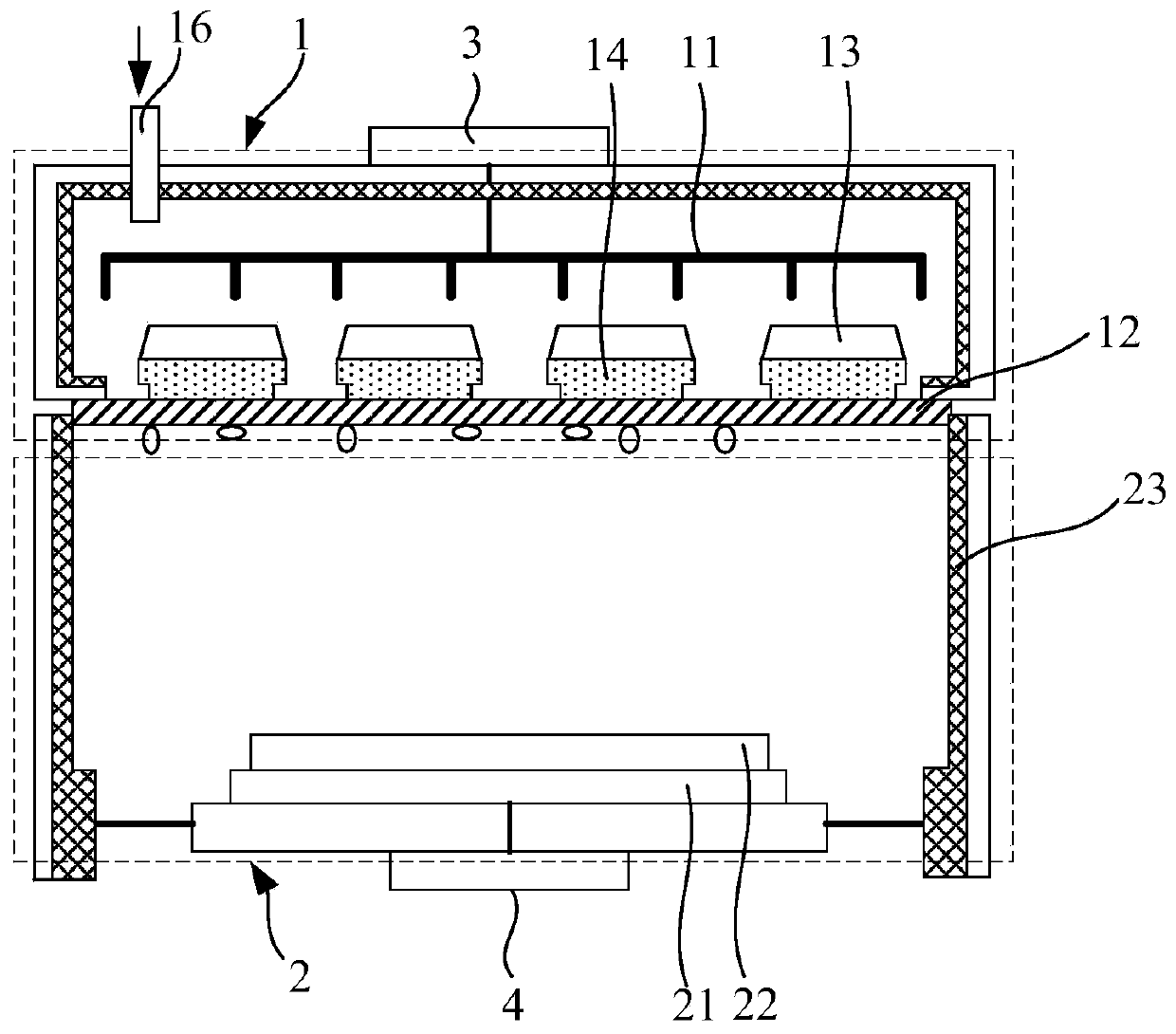
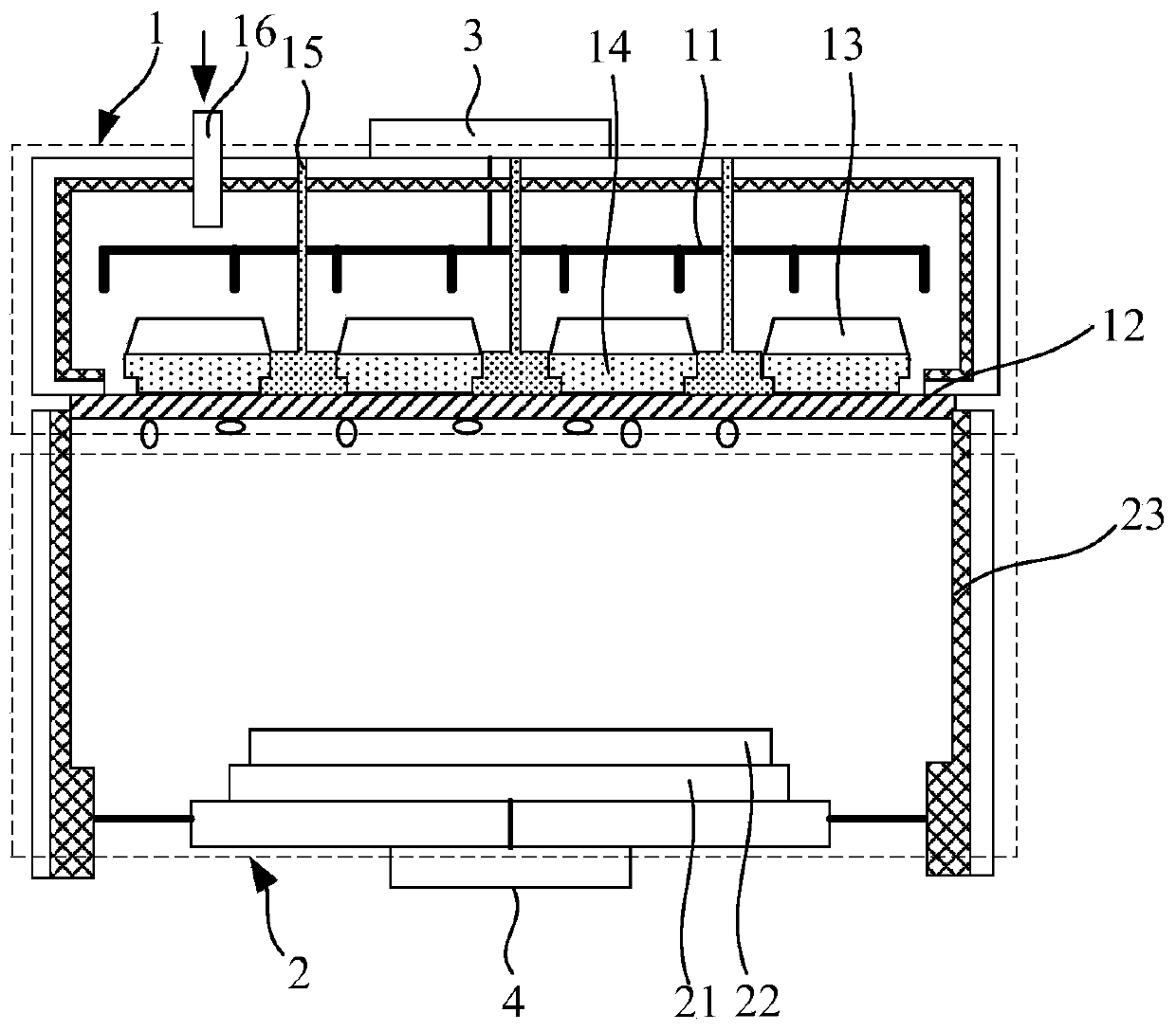
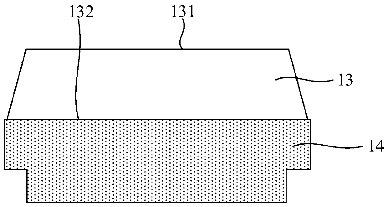
[0028] In order to make the purpose, technical solution and advantages of the present invention clearer, the present invention will be further described in detail below in conjunction with the accompanying drawings, please refer to the drawings in the accompanying drawings, wherein the same component symbols represent the same components, the following description is Based on the particular embodiment of the invention shown, it should not be construed as limiting the invention to other embodiments not detailed herein. The word "embodiment" as used in this specification means an example, instance or illustration.

[0029] In the description of the present application, it should be understood that the terms "center", "longitudinal", "transverse", "length", "width", "thickness", "upper", "lower", "front", " Orientation indicated by rear, left, right, vertical, horizontal, top, bottom, inside, outside, clockwise, counterclockwise, etc. The positional relationship is based on the ...


PUM

PropertyMeasurementUnit
ignition pointaaaaaaaaaa

Abstract

The invention discloses an etching device, which comprises an upper cavity and a lower cavity, and is characterized in that the lower cavity is used for carrying out an etching process on a device. The upper cavity comprises a coil, which is used for bearing alternating current, and an electromagnetic field is generated by the alternating current; electricity inducers which are arranged under thecoil at intervals and used for transmitting the electromagnetic field generated by the coil to the lower cavity; an insulating plate which is arranged at the bottom of the upper cavity and used for preventing plasmas formed by the electromagnetic field from making direct contact with the electricity inducers, and preventing causing corrosion to the electricity inducers and generating arc discharge; and a heating component which is arranged between the insulating plate and the electricity inducers and is used for controlling the temperature of the electricity inducers and the insulating plate.The etching device provided by the embodiment of the invention is used for solving the problem of etching residues caused by adhesion of products in a dry etching process.

Description

technical field [0001] The invention relates to the technical field of semiconductors, in particular to an etching device. Background technique [0002] The etching process is one of the important processes in the manufacturing process of semiconductor devices. It is mainly divided into wet etching using chemical solution for chemical etching and dry etching using initial chemical etching. Among them, dry etching uses corrosive gas or plasma for etching, which can realize anisotropic etching and make the etching pattern finer, and is suitable for fine processes requiring high precision. In the manufacturing process of thin film transistors or organic light emitting diodes, an Inductive Coupled Plasma (ICP) dry etching machine is usually used for the etching process. [0003] However, the thermal conductivity and mechanical strength of the top plate (Top Plate) of the traditional ICP dry etching machine are poor, and its temperature is relatively low compared to other parts ...

Claims


Application Information

Patent Timeline
Patent Type & Authority Applications(China)
IPC IPC(8): H01J37/32H01L21/67
CPCH01J37/32522H01J37/32853H01L21/67069H01J2237/334
Inventor 肖文欢
Owner SHENZHEN CHINA STAR OPTOELECTRONICS SEMICON DISPLAY TECH CO LTD
Why Eureka
Try Eureka