
Capacitor device on chip

A capacitor device and chip technology, applied in the direction of capacitors, circuits, electrical components, etc., can solve problems such as affecting the cost of EEPROM memory

Inactive Publication Date: 2020-04-24
上海明矽微电子有限公司
View PDF0 Cites 0 Cited by
  • Summary
  • Abstract
  • Description
  • Claims
  • Application Information

AI Technical Summary

Problems solved by technology

For example, for EEPROM, a charged erasable programmable read-only memory, a core issue in its design is the area of ​​EEPROM, which directly affects the cost of EEPROM memory

Method used


Image

  • Capacitor device on chip
  • Capacitor device on chip

Examples


Embodiment Construction

[0009] based on the following figure 1 with figure 2 , specifically describe the preferred embodiment.

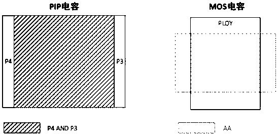
[0010] Such as figure 1 As shown, ordinary capacitors are usually divided into PIP capacitors and MOS capacitors. The PIP capacitor is made of POLY4 and POLY3 as the upper and lower boards; the MOS capacitor is made of AA and POLY as the upper and lower boards.

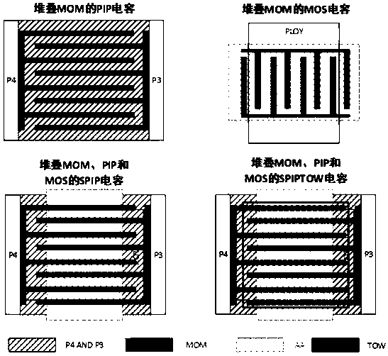
[0011] Such as figure 2 As shown, the present invention proposes multiple methods for superimposing capacitors, which can be combined into four capacitor superimposition methods: MOM+PIP, MOM+MOS, PIP+MOS+MOM, and PIP+MOS+MOM+TOW.

[0012] On the SMIC 0.13um process, the capacitance value of PIP is 2.6fF per square micron; the capacitance value of MOM is 0.5fF per square micron. The capacitance value of PIP+MOM is 3.1fF per square micron, and the unit capacitance value is increased by about 20%.

[0013] Although the content of the present invention has been described in detail through the above preferred e...


PUM


Abstract

At present, the science and technology enter a high-speed development stage, the requirements of people for electronic products are higher and higher, and therefore, higher requirements are raised forchips, namely, higher speed, smaller area, and lower efficiency. For example, for an electrically erasable programmable read-only memory (EEPROM), the core problem of the design is the area of the EEPROM which directly influences the cost of the EEPROM. Under the same process, if the area can be minimized and the performance is good, a relatively large area cost advantage can be achieved. Effortsneed to be made in many aspects in order to reduce the area of the EEPROM, such as simplified design, reasonable layout of modules, use of stacked capacitors and the like. The invention provides a stacked capacitor device. The area and the cost of a chip are remarkably reduced under the condition of not increasing the mask level and the production cost of the chip.

Description

technical field [0001] The present invention belongs to the technical field of integrated circuits, specifically, to the technical field of chip design. Background technique [0002] Chips are widely used in many different fields. With the development of electronic information, the integration of the system is getting higher and higher. In the field of electronic information, embedded chips are widely used: such as single-chip microcomputer, DSP, smart card, etc.; there are storage chips: such as FLASH, EEPROM, etc. [0003] With the growth of emerging industries such as mobile Internet, cloud computing, Internet of Things, and big data, the electronic information industry has entered a new stage of development. Control, communication, automotive electronics, human-computer interaction, and network interconnection have incorporated a large number of emerging electronic technologies. The functions of equipment are becoming more and more complex, and the degree of system inte...

Claims


Application Information

Patent Timeline
IPC IPC(8): H01L49/02
CPCH01L28/40
Inventor 韦强张建伟
Owner 上海明矽微电子有限公司
Learn More