Annealing treatment method and device for reducing internal stress of crystal

An annealing treatment and internal stress technology, applied in the directions of post-processing, crystal growth, post-processing details, etc., can solve the problems of reducing the productivity of the crystal growth furnace, cannot be eliminated, and the radial temperature gradient of the crystal cannot be changed, so as to solve the cracking of the crystal ingot , Reduce radial stress and eliminate residual thermal stress

Active Publication Date: 2020-04-28
SICC CO LTD
View PDF5 Cites 9 Cited by
  • Summary
  • Abstract
  • Description
  • Claims
  • Application Information

AI Technical Summary

Problems solved by technology

The number of top heaters is 1 or 2, and the power of the appropriate top heater is set to make the temperature at the center of the crystal higher than the temperature at the edge, or to make the temperature at the top of the crystal higher than the temperature at the bottom, but the radial temperature gradient of the crystal cannot be changed or eliminated , the intelligent control of the temperature gradient cannot be realized, and the stress inside the crystal cannot be completely eliminated, and the device is used for in-situ annealing of the crystal, which will reduce the productivity of the crystal growth furnace

Method used


Image

  • Annealing treatment method and device for reducing internal stress of crystal
  • Annealing treatment method and device for reducing internal stress of crystal
  • Annealing treatment method and device for reducing internal stress of crystal

Examples


Embodiment 1

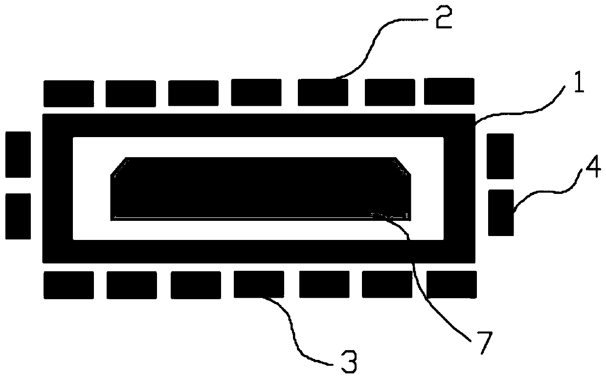
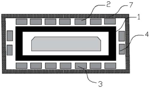
[0050] Embodiment 1: The present invention is used for the device of silicon carbide crystal annealing treatment, and its specific structure is as follows:

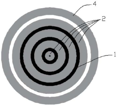
[0051] Such as Figure 1~3 As shown, the device for crystal annealing treatment of the present invention includes a crucible 1 and a heating device for heating the crucible 1, and the heating device includes a plurality of first heating rings 2 distributed above the crucible 1, and a plurality of first heating rings 2 distributed below the crucible. A plurality of second heating rings 3, and a plurality of third heating rings 4 arranged on the side of the crucible; wherein the plurality of first heating rings 2 are concentrically arranged with the upper center of the crucible 1 as the center, and the plurality of second heating rings 3 The crucible 1 is set concentrically with the center below the center of the crucible 1 , and the first heating ring 2 and the second heating ring 3 are symmetrically set.

[0052] In the ...

Embodiment 2

[0063] Embodiment 2: the annealing treatment method of crystal

[0064] According to an embodiment of the present application, a method for crystal annealing using the device described in Example 1 includes:

[0065] (1) Preparatory stage: Put the crystal (6 inches) to be annealed into crucible 1, vacuumize and feed inert gas (Ar gas), so that the pressure in crucible 1 is controlled at 200-900mbar, and the flow rate of Ar gas is controlled at 50- 500ml / min;

[0066] (2) Heating stage: if Figure 4 As shown, simultaneously control all heating rings (first heating rings A1, A2, A3, A4, second heating rings B1, B2, B3, B4, third heating rings S1, S2) to start synchronous heating, and heat to T1 (1700 ~2300℃), keep warm for 1~10h;

[0067] During the crystal growth process, the temperature of the growth surface is higher than that of the seed crystal plane, and the temperature of the crystal center on the same plane is lower than that of the crystal edge. Therefore, at this s...


PUM


Abstract

The invention provides an annealing treatment method for reducing the internal stress of a crystal. The annealing treatment method comprises the following steps: (1) a preparation stage: putting the crystal to be annealed into a crucible, vacuumizing the crucible, and introducing inert gas; and (2) a heating stage: heating the crucible by using a heating device, and in the heating process, respectively controlling the heating temperatures of a plurality of first heating rings concentrically arranged above the crucible in the heating device so that the crucible forms a radial temperature gradient. The heating temperature of a plurality of first heating rings of the heating device is controlled, the crucible forms the radial temperature gradient, the radial temperature gradient different from or opposite to the radial temperature gradient during crystal growth can be obtained and radial stress of the crystal can be remarkably reduced. The heating temperature of the first heating ring below the crucible and the heating temperature of the third heating ring on the side face of the crucible are controlled, the axial temperature gradient of the crucible is achieved, the axial temperaturegradient different from or opposite to the axial temperature gradient of the crystal in the growth process can be obtained and basic elimination of residual thermal stress can be achieved.

Description

technical field [0001] The invention relates to an annealing treatment method and device for reducing internal stress of crystals, and belongs to the technical field of annealing treatment after crystal growth is completed. Background technique [0002] Silicon carbide is one of the third-generation wide-bandgap semiconductor materials after silicon and gallium arsenide. Widely used in power electronics, radio frequency devices, optoelectronic devices and other fields. High-quality crystals are the cornerstone of the development of semiconductor and information industries, and their preparation level restricts the preparation and performance of downstream devices. Although physical meteorological transport (PVT) growth of silicon carbide crystals has made great progress in recent years, for large-size single-crystal silicon carbide, excessive residual stress is an urgent problem to be solved, especially for ≥6-inch If the silicon carbide single crystal is too high, too muc...

Claims


Application Information

Patent Timeline
Patent Type & Authority Applications(China)
IPC IPC(8): C30B33/02C30B29/36
CPCC30B29/36C30B33/02
Inventor 方帅高宇晗高超李霞宁秀秀王路平张九阳王宗玉潘亚妮舒天宇
Owner SICC CO LTD
Why Eureka
Try Eureka