Transfer printing process method for flexible MEMS device

A process method and flexible technology, applied in the field of semiconductor/MEMS manufacturing process, can solve the problems of high requirements for accurate transfer temperature and time, long release time, device structure failure, etc., so as to shorten the release time and improve the transfer rate. Success rate, the effect of enhancing adhesion

Active Publication Date: 2020-05-01
DALIAN UNIV OF TECH
View PDF13 Cites 8 Cited by
  • Summary
  • Abstract
  • Description
  • Claims
  • Application Information

AI Technical Summary

Problems solved by technology

[0004] The thermal release tape transfer method has high requirements on the precise grasp of the transfer temperature and time; the water-soluble tape will decompose when it meets water, but a small amount of residue remains on the surface of the structure, polluting the structure; PDMS is the most widely used in the flexible transfer process stamp material, the process is the most feasible, but the traditional transfer process often uses SiO 2 In order to release the sacrificial layer of the process, it was found in many experiments that SiO 2 When used as a sacrificial layer, the release time is too long, causing the device structure to fail due to too long soaking time in HF acid buffer, and the adhesion between the device and the flexible acceptor substrate is too weak during the printing process

Method used


Image

  • Transfer printing process method for flexible MEMS device
  • Transfer printing process method for flexible MEMS device

Examples


specific Embodiment approach

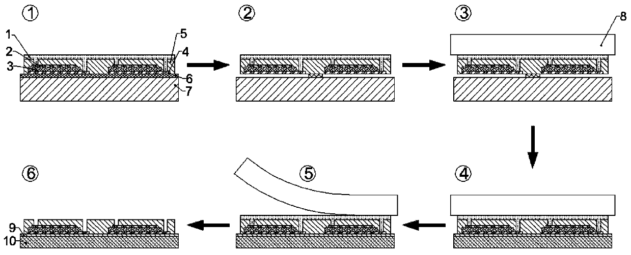
[0021] A transfer printing process method for flexible MEMS devices, the specific steps are as follows:

[0022] Step one, such as figure 1 As shown in step ①, a layer of SiN is deposited on the cleaned 2-inch single crystal silicon wafer by PECVD X sacrificial layer film, where NH 3 and SiH 4 The feeding ratio of the solution is 8:1, the reaction temperature is 450°C, the reaction pressure is 160Pa, and the deposition rate is 1nm / s. Measure its thickness after deposition, in this example SiN X The thickness of the sacrificial layer is 0.8 μm;

[0023] Step two, such as figure 1 As shown in step ①, the SiN X Make bottom electrode Ti(50nm) / Pt(200nm)-PZT(500nm)-top electrode Cr(10nm) / Au(100nm) three-layer device structure on the sacrificial layer, spin coating (low speed 600r / min, gluing time 9s, high speed 3000r / min, gluing time 30s), pre-baking (temperature 120°C, time 3min), nitrogen oven curing (curing by step drying, the temperature is 50°C, 30min, 140°C, 30min, 350...


PUM

PropertyMeasurementUnit
thicknessaaaaaaaaaa
thicknessaaaaaaaaaa

Abstract

The invention belongs to the technical field of semiconductor / MEMS manufacturing processes, provides a transfer printing process method for a flexible MEMS device, and particularly can be used for transferring a structure or device manufactured on a rigid substrate such as silicon onto a flexible substrate such as polyimide, PET and PDMS. In a case of a PZT-based flexible piezoelectric energy collector, aiming at the problem that the success rate of the whole process is affected due to low success rate of the process, the invention innovatively proposes the use of SiNX deposited by PECVD as asacrificial layer released before transfer printing. Compared with a sacrificial layer taking SiO2 as a release process in a traditional process, the improvement obviously shortens the release time, so that the structure is prevented from losing efficacy due to long-time soaking in an HF acid buffer solution, and the success rate of a transfer printing process is greatly improved. And meanwhile, the process improvement of pressurizing and heating in the transfer printing period is provided, and the transfer printing success rate is further increased.

Description

technical field [0001] The invention belongs to the technical field of semiconductor / MEMS manufacturing technology, and is a process method for improving the success rate of multi-layer microstructure transfer printing by improving sacrificial layers and process conditions, and is applicable to the transfer printing process flow of flexible MEMS devices. Background technique [0002] Extensible flexible MEMS electronic devices combine inorganic electronic materials with flexible substrates, which not only maintains the superior electrical properties of inorganic electronic materials, but also has good ductility. It has a wide range of applications in the fields of display, energy, medical health, and human-computer interaction. Application prospects. However, inorganic electronic materials cannot be directly grown and processed on flexible substrates. To solve this problem, researchers have developed transfer printing technology, which peels inorganic thin films from their g...

Claims


Application Information

Patent Timeline
Patent Type & Authority Applications(China)
IPC IPC(8): B81C1/00
CPCB81C1/00134B81C1/00476
Inventor 崔岩高志东李嘉豪于舜尧
Owner DALIAN UNIV OF TECH
Why Eureka
Try Eureka