Ultraviolet LED packaging structure
A technology of LED packaging and LED chips, which is applied in the direction of electrical components, circuits, semiconductor devices, etc., can solve problems such as poor reliability, achieve the effects of reducing irradiation, reducing comprehensive stress, and preventing metal atom migration
- Summary
- Abstract
- Description
- Claims
- Application Information
AI Technical Summary
Problems solved by technology
Method used
Image

Examples
Embodiment 1
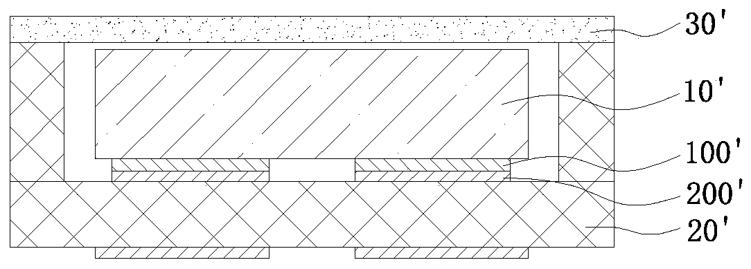
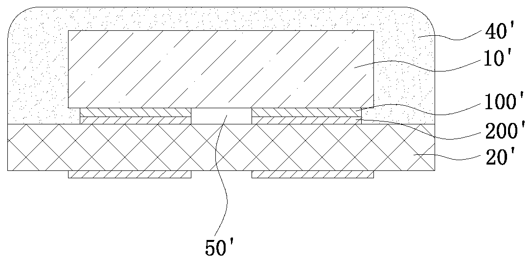
[0038] like image 3 As shown, this embodiment provides an ultraviolet LED packaging structure, which includes an ultraviolet LED chip 10 in a flip-chip structure, a packaging substrate 20 and an encapsulating adhesive 40 covering the ultraviolet LED chip 10 . The wavelength of the LED chip 10 can be between 200-380nm, and the light-emitting wavelength can be selected according to the needs of practical applications, such as surface sterilization and surface curing. Preferably, the LED chip 10 is 200-340nm.
[0039] Wherein, the ultraviolet LED chip 10 is a flip-chip structure, and there are two chip electrodes 100 as positive and negative electrodes on the bottom surface away from the light-emitting surface. The packaging substrate 20 can be ceramic materials such as aluminum nitride and aluminum oxide, preferably aluminum nitride ceramic materials with a larger thermal conductivity. The packaging substrate 20 has at least two substrate electrodes 200 matched with the chip e...
Embodiment 2
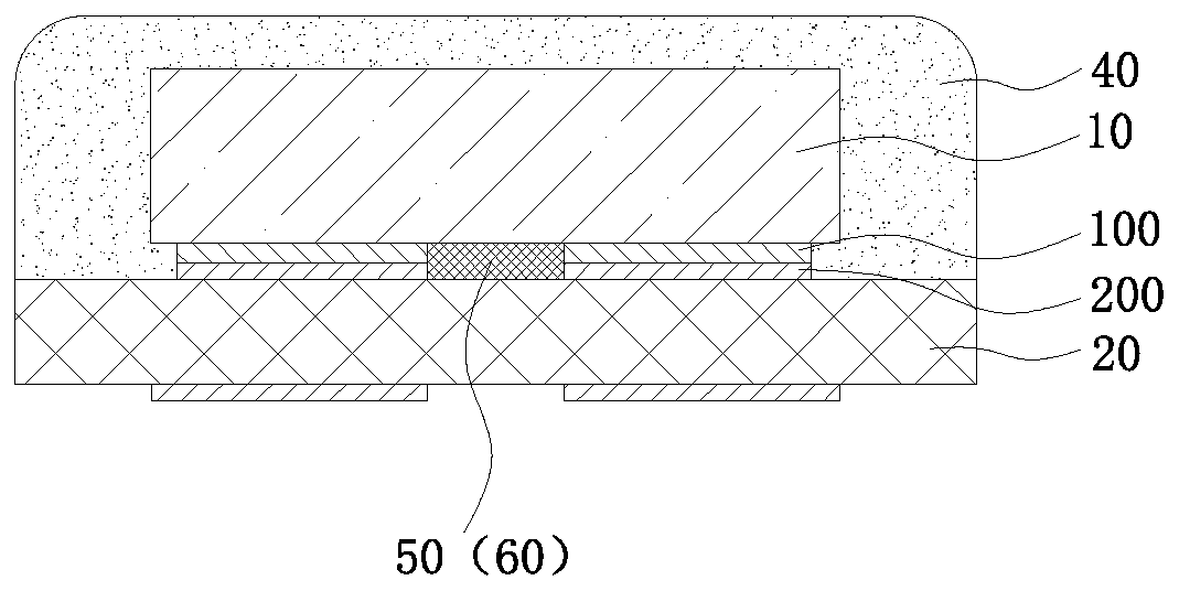
[0051] like Figure 7 and Figure 8 As shown, this embodiment also provides an ultraviolet LED packaging structure, which is roughly the same as the ultraviolet LED packaging structure in Embodiment 1, the difference is that the packaging glue of the ultraviolet LED packaging structure in this embodiment The packaging methods of the material 40 are different.
[0052] The packaging adhesive 40 of the ultraviolet LED packaging structure in this embodiment is completely coated on the surface of the package along the surface of the chip and the surface of the ceramic substrate by vacuum filming. Since the surface of the ceramic substrate in contact with the fluororesin itself has metal bumps, And inherent LED chips or other components, the surface is uneven, so the packaging structure after vacuum coating forms a concave-convex curved surface structure. The thickness of the fluororesin film of this structure should be smaller than that of the LED chip, preferably, the film thic...
PUM
| Property | Measurement | Unit |
|---|---|---|
| thickness | aaaaa | aaaaa |
| emission peak | aaaaa | aaaaa |
| crystallinity | aaaaa | aaaaa |
Abstract
Description
Claims
Application Information
 - R&D
- Intellectual Property
- Life Sciences
- Materials
- Tech Scout
- Unparalleled Data Quality
- Higher Quality Content
- 60% Fewer Hallucinations
Browse by: Latest US Patents, China's latest patents, Technical Efficacy Thesaurus, Application Domain, Technology Topic, Popular Technical Reports.
© 2025 PatSnap. All rights reserved.Legal|Privacy policy|Modern Slavery Act Transparency Statement|Sitemap|About US| Contact US: help@patsnap.com