Positive and negative sample data balancing method in factory PCB defect detection

A PCB board and defect detection technology, applied in the field of data processing, can solve problems such as model overfitting, positive and negative sample imbalance, etc., and achieve the effect of strong robustness, broad market application prospects, and superior synthesis effect

Pending Publication Date: 2020-05-08
FOSHAN NANHAI GUANGDONG TECH UNIV CNC EQUIP COOP INNOVATION INST +1
View PDF3 Cites 6 Cited by
  • Summary
  • Abstract
  • Description
  • Claims
  • Application Information

AI Technical Summary

Problems solved by technology

In the PCB defect detection project, the number of negative samples with defects is only a thousand, while the number of positive samples without defects is on the order of 100,000. It can be seen

Method used


Image

  • Positive and negative sample data balancing method in factory PCB defect detection
  • Positive and negative sample data balancing method in factory PCB defect detection
  • Positive and negative sample data balancing method in factory PCB defect detection

Examples


Embodiment 1

[0053] Such as Figure 1 to Figure 5 As shown, the present embodiment discloses a positive and negative sample data balance method in a factory PCB board defect detection, and the balance method mainly includes the following specific steps:

[0054] 1) Collect, organize and classify data sets: collect image data sets of factory PCB boards, organize the data sets, and manually classify according to whether there are defects.

[0055] Specifically, in step 1) data preprocessing needs to set specific and clear classification rules, and the classification boundaries cannot be blurred. A positive sample refers to a PCB without defects, and a negative sample refers to a defective PCB.

[0056] Preferably, for simplicity, the input images are all regularized to a size of 256*256.

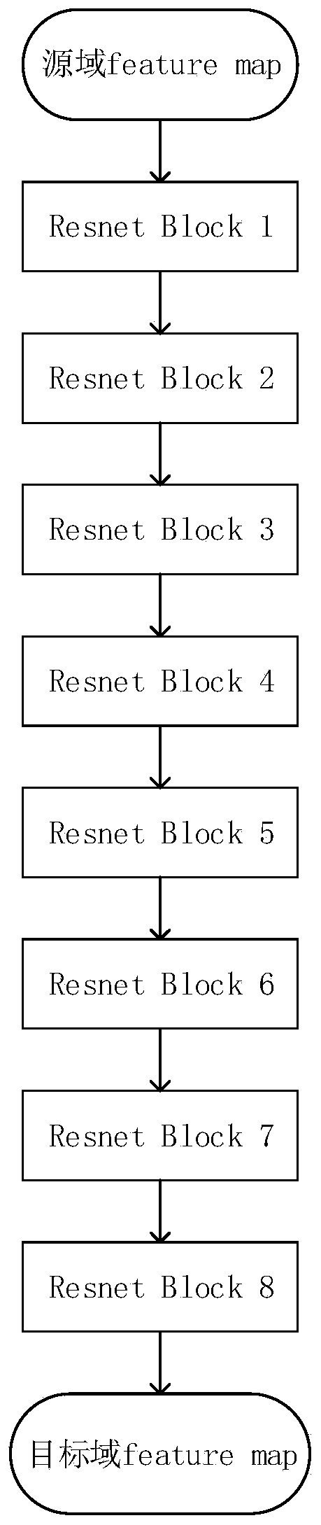
[0057] 2) Construct a generative adversarial network model to solve the problem of imbalance between positive and negative samples, aiming to design a network structure based on two groups of unidirectio...

Embodiment 2

[0077] combine Figure 1 to Figure 8 As shown, this embodiment discloses a method for balancing positive and negative sample data in a factory PCB board defect detection, including the following specific implementation steps:

[0078] 1) Collect the image data set of the PCB board in the factory, organize the data set, and manually classify it according to whether there are defects.

[0079] 2) Construct a generative adversarial network model to solve the problem of imbalance between positive and negative samples. The envisaged method is unsupervised image-to-image translation, aiming to design a network structure based on two sets of unidirectional GANs and achieve bidirectional image generation.

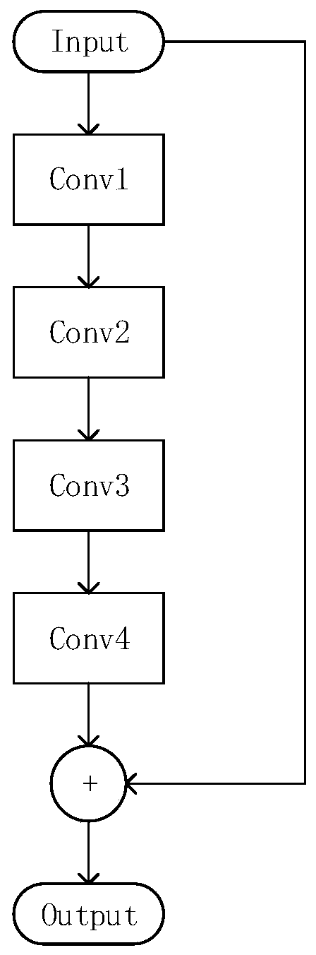
[0080] 3) The model is divided into generator and discriminator. Firstly, the generator module is designed. Generators include encoders, converters and decoders.

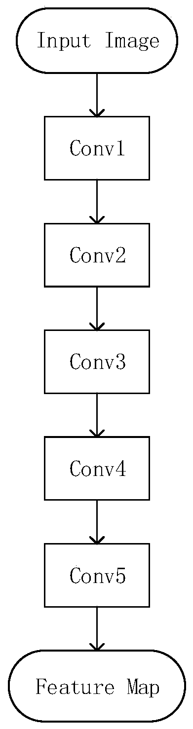
[0081] 4) Design of the encoder. Different channels of the encoder output feature map combine different features ...


PUM


Abstract

The invention discloses a positive and negative sample data balancing method in factory PCB defect detection, which is a data balancing method in PCB positive and negative sample classification basedon an adversarial generative network, and mainly comprises the following steps: collecting, sorting and classifying a data set; designing an encoder which is composed of five convolution layers, and extracting features from the input image by the encoder; designing a converter which is composed of eight residual blocks and converts the feature vector from a source domain to a target domain; designing a decoder, wherein the decoder is composed of five deconvolution layers; designing a discriminator, wherein the discriminator is composed of seven convolution layers; designing a loss function, wherein the loss function comprises four parts; preparing a training set for model training; the obtained weight file is used for a test set, and a negative sample needing to be amplified is synthesized. The method is high in robustness, wide in application range and excellent in synthesis effect. And by means of cyclic consistency conditions, the effect of standardizing the model is achieved, and the generation effect of the shape and texture of the synthesized image is flexibly controlled to a certain extent.

Description

technical field [0001] The invention relates to the technical field of data processing, in particular to a method for balancing positive and negative samples in a factory assembly line product based on an adversarial generation network. Background technique [0002] Printed Circuit Board (PCB) welding machines are mainly used on equipment in the electronics industry. The industry has higher quality requirements for PCB boards. Therefore, the quality of PCB boards needs to be tested. PCB board has the characteristics of high density, high precision and high reliability. As the number of PCB board layers increases, the density increases, and the volume of the PCB board decreases, making it more difficult to inspect the quality of the PCB board. [0003] In the production line, due to reasons such as immature welding technology and manual operation errors, quality problems such as welding defects often occur, which greatly affect the use of products. [0004] In the past, aut...

Claims


Application Information

Patent Timeline
IPC IPC(8): G06K9/62G06N3/04G06N3/08G06T7/00
CPCG06T7/0004G06N3/08G06T2207/20084G06T2207/20081G06N3/045G06F18/24G06F18/214
Inventor 黄坤山史扬艺
Owner FOSHAN NANHAI GUANGDONG TECH UNIV CNC EQUIP COOP INNOVATION INST
Why Eureka
Try Eureka