CMOS image sensor structure and manufacturing method

An image sensor and pixel unit technology, applied in the direction of electric solid-state devices, semiconductor devices, radiation control devices, etc., can solve the problems of over-corrosion, affecting device characteristics, and the end point of corrosion stop is not easy to control, etc., to achieve low power consumption, high The effect of integration

Pending Publication Date: 2020-05-08
SHANGHAI INTEGRATED CIRCUIT RES & DEV CENT +1
View PDF4 Cites 1 Cited by
  • Summary
  • Abstract
  • Description
  • Claims
  • Application Information

AI Technical Summary

Problems solved by technology

Since the doping concentrations of the highly doped substrate 15 and the device silicon layer 14 are different, their corresponding etching rates are also different, so the etching process is mainly stopped by the different etching rates between the two, but the difference in doping concentration The resulting difference in corrosion rate is small, so the end point of corrosion stop is not easy to control, often causing over-corrosion phenomenon; at the same time, the impurity concentration in the highly doped substrate 15 is relatively high, and it is easy to precipitate during the high temperature process, thereby affecting device characteristics

Method used


Image

  • CMOS image sensor structure and manufacturing method
  • CMOS image sensor structure and manufacturing method
  • CMOS image sensor structure and manufacturing method

Examples


Embodiment Construction

[0048] The specific embodiment of the present invention will be further described in detail below in conjunction with the accompanying drawings.

[0049] It should be noted that, in the following specific embodiments, when describing the embodiments of the present invention in detail, in order to clearly show the structure of the present invention for the convenience of description, the structures in the drawings are not drawn according to the general scale, and are drawn Partial magnification, deformation and simplification are included, therefore, it should be avoided to be interpreted as a limitation of the present invention.

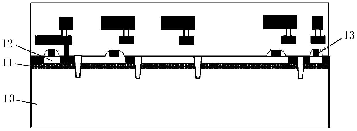
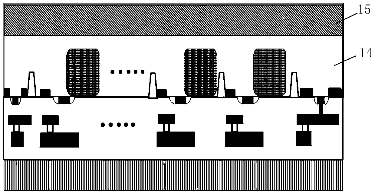
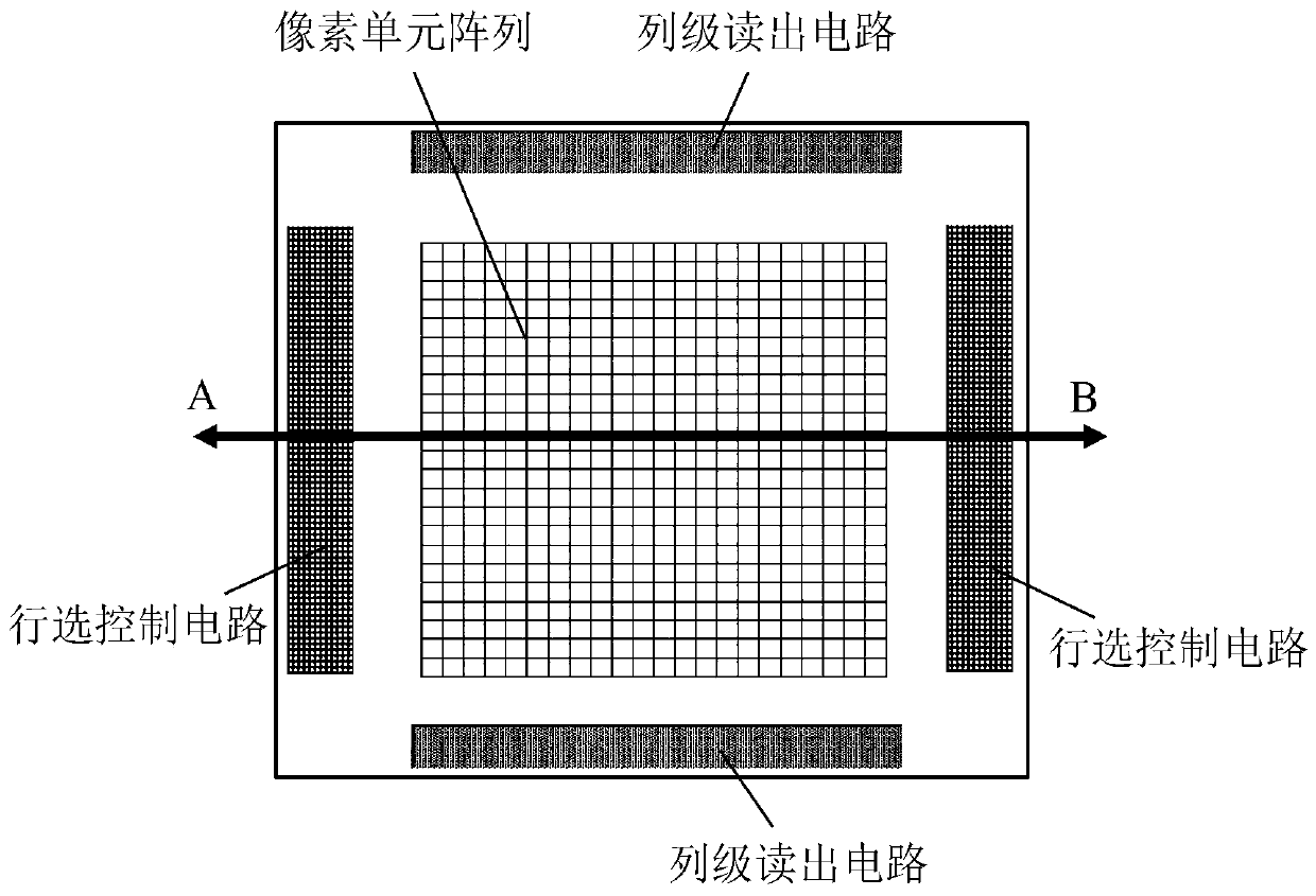
[0050] In the following specific embodiments of the present invention, please refer to Figure 3-Figure 4 , image 3 It is a schematic layout diagram of a CMOS image sensor chip, Figure 4 is along image 3 A schematic diagram of a cross-sectional structure of a CMOS image sensor in a preferred embodiment of the present invention at the position A...


PUM


Abstract

The invention discloses a CMOS image sensor structure. The structure is arranged on a first silicon substrate and a second silicon substrate which are stacked up and down, the first silicon substratecomprises a first buried oxide layer and a first silicon layer arranged below the first buried oxide layer, the second silicon substrate comprises a second buried oxide layer and a second silicon layer arranged below the second buried oxide layer, the thickness of the first silicon layer is greater than that of the second silicon layer, the first silicon layer is bonded with the second buried oxide layer, a through opening is formed on the second silicon substrate corresponding to the pixel unit array area, a plurality of photosensitive parts and control transistors of the pixel unit array arearranged on the back surface of the first silicon layer corresponding to the position of the opening, and peripheral circuit transistors are arranged on the back surface of the second silicon layer around the opening. According to the invention, the manufacturing of the pixel unit of the backside illuminated image sensor can be realized while a low-power SOI device is used in a peripheral circuit, and the problems of impurity self-doping and poor thickness uniformity after thinning easily caused by a conventional backside illuminated process can be avoided.

Description

technical field [0001] The invention relates to the technical field of semiconductor processing, in particular to a CMOS image sensor structure and a manufacturing method. Background technique [0002] For half a century, the semiconductor industry has been shrinking transistor size, increasing transistor density, and improving performance in accordance with Moore's Law. However, as the size of bulk silicon transistor devices with planar structure is getting closer and closer to the physical limit, Moore's law is getting closer and closer to its end; therefore, some new structures of semiconductor devices called "non-classical CMOS" have been proposed . These technologies include FinFET, carbon nanotubes, silicon on insulator (silicon on insulator, SOI), silicon germanium on insulator (SiGe on insulator, SiGeOI) and germanium on insulator (Ge on insulator, GeOI), etc. [0003] Through these new structures, the performance of semiconductor devices can be further improved. ...

Claims


Application Information

Patent Timeline
IPC IPC(8): H01L27/146
CPCH01L27/1464H01L27/14643H01L27/14601H01L27/14689
Inventor 顾学强张美丽奚鹏程
Owner SHANGHAI INTEGRATED CIRCUIT RES & DEV CENT
Why Eureka
Try Eureka