Heating film and method for manufacturing same
A manufacturing method and technology of heating film, applied in ohmic resistance heating, chemical instruments and methods, transparent/reflective heating devices, etc., can solve the problems of complex structure, increased haze of film and bonded glass, affecting physical properties of laminated glass, etc. , to achieve the effect of low reflectivity and low cost
- Summary
- Abstract
- Description
- Claims
- Application Information
AI Technical Summary
Problems solved by technology
Method used
Image
Examples
Embodiment 1
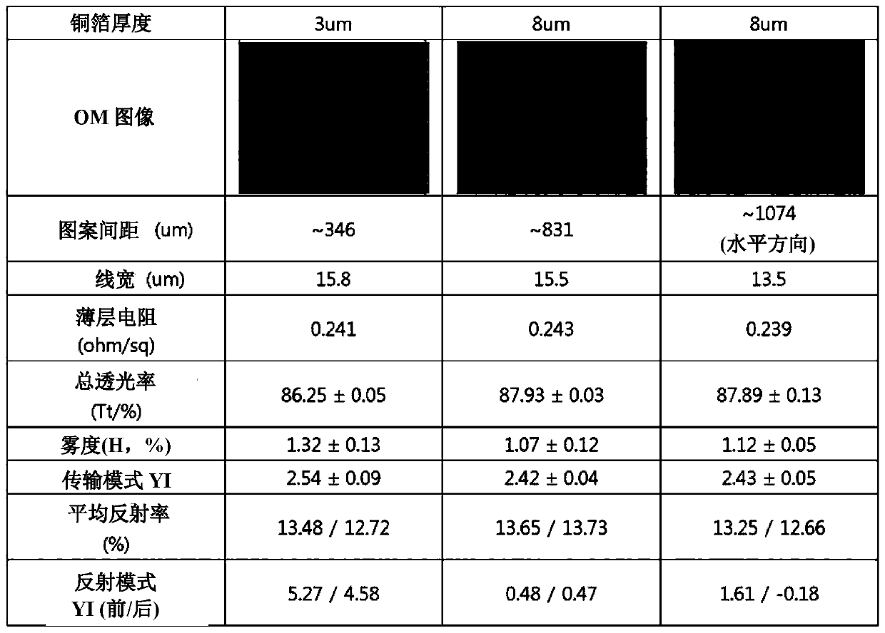
[0102] Coating thickness of 3 μm and 8 μm matte surface of copper foil, and then dried at 120° C. for 10 minutes to form a PVB layer with a thickness of 5 μm to 7 μm on the matte surface of copper foil. In this case, the Rz of the matte surface of the 3 μm copper foil was 1.5 μm, and the Rz of the matte surface of the 8 μm copper foil was 1.63 μm. Meanwhile, for a copper foil of 3 μm, the average reflectance of the matte surface measured at a wavelength of 380nm to 780nm is 7.6%.
[0103] Afterwards, the substrate was fabricated by laminating PET with a thickness of 50 μm on the copper foil PVB surface at 80 °C and a speed of 4 mpm. In the case of the copper foil having a thickness of 3 μm, since the carrier foil having a thickness of 18 μm was attached to the rear surface of the copper foil to facilitate operation of the film process, the carrier foil was removed before patterning. After that, the copper foil was cleaned / washed / dried with 0.5 wt% sulfuric acid, and then a d...
Embodiment 2
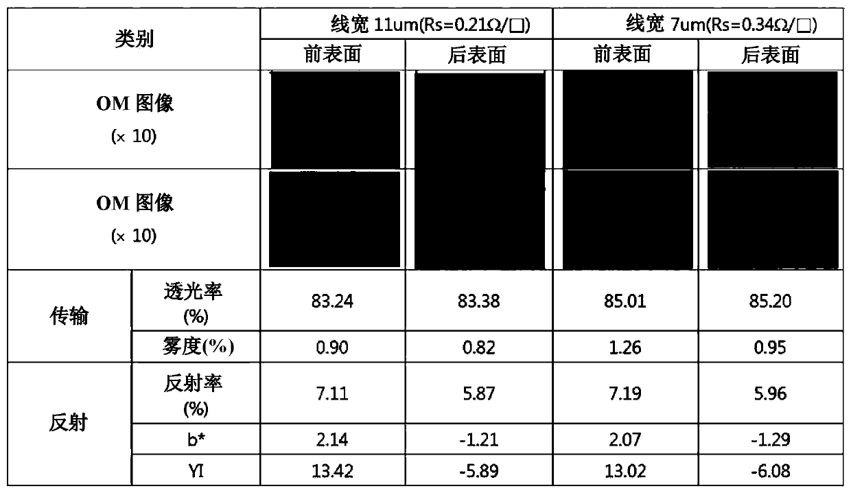
[0106] A coating solution having a refractive index of 1.47 and a glass transition temperature (Tg) of 32° C., 43 parts by weight of ethanol, and 43 parts by weight of methyl ethyl ketone was used to coat a film having a thickness of 3 μm. Copper foil with a matte surface, then dried at 120°C for 3 minutes, and then, after forming a PVB layer with a thickness of 5 μm to 7 μm, thermally laminated with PET with a thickness of 50 μm at 110°C by a hot roll laminator to manufacture substrate. In this case, the matte surface of the 3 μm copper foil used had a surface roughness Rz of 1.5 μm, and an average reflectance measured at a wavelength of 380 nm to 780 nm was 6.7%. In the case of the copper foil having a thickness of 3 μm, since the carrier foil having a thickness of 18 μm was attached to the rear surface of the copper foil to facilitate operation of the film process, the carrier foil was removed before patterning. Form a novolac resin-based resist pattern with a thickness of...
Embodiment 3
[0109]For a copper foil having a thickness of 3 μm, in which the surface roughness of the matte surface is 1.5 μm and the average reflectance measured for the surface at a wavelength of 380 nm to 780 nm is 6.7%, the refractive index with a composition of 14 parts by weight is 1.47 and a glass transition temperature (Tg) of 32° C. PVB, 43 parts by weight of ethanol and 43 parts by weight of methyl ethyl ketone coating solution coated with a thickness of 3 μm copper foil matte surface, and then at 120 °C for 3 minutes to form a PVB layer with a thickness of 5 μm to 7 μm. After that, for the film that was subjected to the process of PET lamination and removal of the carrier foil with a thickness of 18 μm on the back side in the same manner as in Example 2, a resist pattern was formed, and copper was etched, and the resist was removed with a 3% NaOH aqueous solution, The air-exposed copper surface was then blackened by dipping the film in a selenium-based blackening solution for 3...
PUM
| Property | Measurement | Unit |
|---|---|---|
| thickness | aaaaa | aaaaa |
| thickness | aaaaa | aaaaa |
| thickness | aaaaa | aaaaa |
Abstract
Description
Claims
Application Information


