Nano-conductor or semiconductor material size-controllable preparation system and preparation method

A preparation system and technology of nanomaterials, applied in the preparation system and field of nanoconductor or semiconductor materials with controllable size, can solve problems such as sustainable control of difficult reaction processes, difficulty in controlling size, difficulty in obtaining nanoparticles, etc., to achieve Stable and controllable processing, reduced transfer, good monodispersity

Active Publication Date: 2020-10-27
GUANGDONG UNIV OF TECH
View PDF6 Cites 0 Cited by
  • Summary
  • Abstract
  • Description
  • Claims
  • Application Information

AI Technical Summary

Problems solved by technology

[0003] At present, there are two types of chemical methods and physical methods for controlling the size of nanoconductors or semiconductor materials. Most of the chemical methods use liquid phase reactions to control the size of nanoconductors or semiconductor materials. However, liquid phase reactions are related to A series of factors such as the concentration of reactants, reaction temperature, and reaction time make it difficult to sustainably control the entire reaction process.
The physical law is to prepare nanoconductors or semiconductor materials of different sizes by adding suitable precipitants in the sol-gel method, controlling the pH value of the system and the relative ratio of water or surfactants in the microemulsion method, etc., but in the size It is difficult to control, and it is difficult to accurately obtain nanoparticles with uniform particle size

Method used


Image

  • Nano-conductor or semiconductor material size-controllable preparation system and preparation method
  • Nano-conductor or semiconductor material size-controllable preparation system and preparation method
  • Nano-conductor or semiconductor material size-controllable preparation system and preparation method

Examples


Embodiment Construction

[0028] The technical solutions of the present invention will be further described below in conjunction with the accompanying drawings and through specific implementation methods.

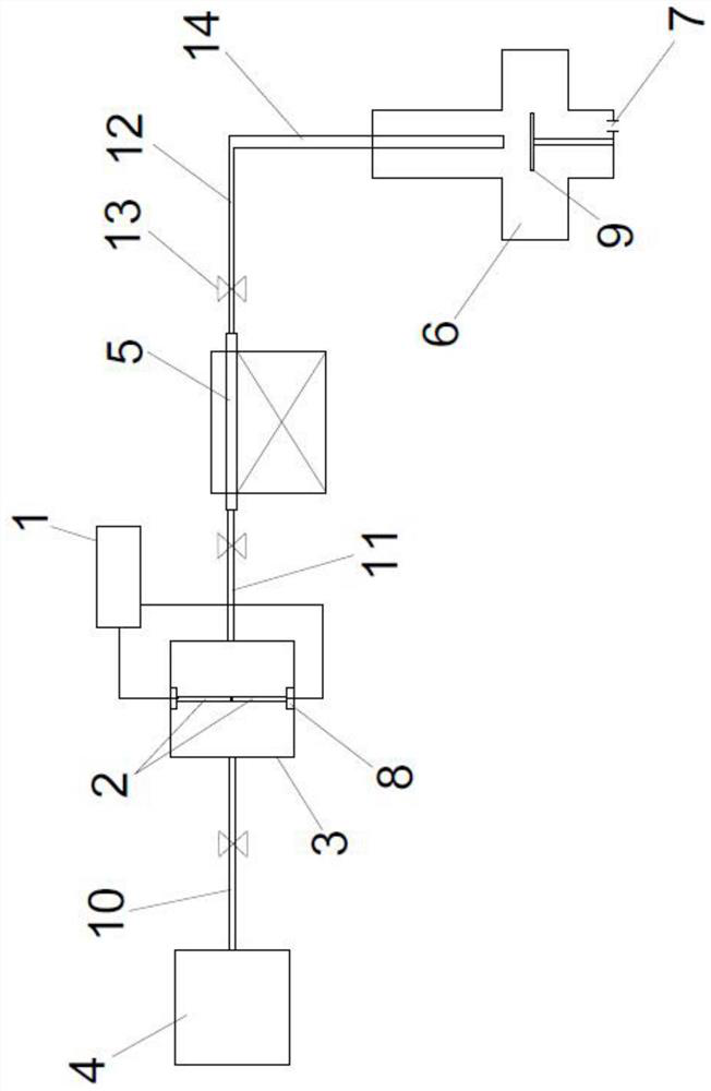
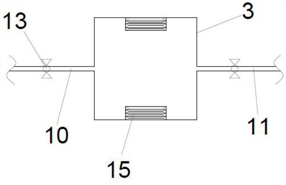
[0029] Such as Figure 1-4 As shown, the size-controllable preparation system of nano-conductor or semiconductor material includes a nano-material preparation device, a size control device and a collection device connected in sequence. The nano-material preparation device consists of a power supply 1, an electrode 2, an ablation reaction vessel 3 and Composed of an inert gas source 4, the size control device is a tube furnace 5 for heat-treating nanoconductor or semiconductor materials, the collection device includes a collection box 6, and the inert gas source 4 communicates with the ablation reaction vessel 3. The ablation reaction container 3 is connected to the tube furnace 5, and the tube furnace 5 is connected to the collection box 6, and the bottom of the collection box 6 is provided with an ...


PUM

PropertyMeasurementUnit
particle sizeaaaaaaaaaa

Abstract

The invention discloses a preparation system and a preparation method with controllable size of nano conductor or semiconducting material, including a nano material preparation device, a size control device and a collection device connected in sequence, the nano material preparation device consists of a power supply, an electrode, an ablation reaction vessel and an inert Composed of gas sources, the size control device is a tube furnace for heat treatment of nano conductors or semiconductor materials, the collection device includes a collection box; there are two electrode holders for installing fixed electrodes in the ablation reaction container, two The electrode fixing seats are oppositely arranged on the inner wall of the ablation reaction vessel, and the two electrode fixing seats are respectively electrically connected to the two poles of the power supply. By adjusting the temperature in the tube furnace in the size control device, the length of the tube furnace, and the speed at which the nano conductor or semiconductor material passes through the tube furnace with the inert gas, the heat treatment temperature and temperature of the nano conductor or semiconductor material in the tube furnace can be changed. The heat treatment time, thereby controlling the final size of the nanoconductor or semiconductor material.

Description

technical field [0001] The invention relates to the technical field of preparation of nanometer materials, in particular to a preparation system and a preparation method with controllable size of nanometer conductor or semiconductor material. Background technique [0002] Due to their basic characteristics such as small size effect, surface interface effect, and quantum size effect, nanoconductor or semiconductor materials exhibit physical and chemical properties different from macroscopic bulk materials, and have great potential in the fields of electronics, catalysis, lubrication, antibacterial, and biomedicine. application prospects. In particular, the preparation of nanoconductors or semiconductor materials with different sizes has been widely concerned, because nanoconductors or semiconductor materials with different sizes have significant differences in material properties, which have great influence on the optical, electrical, magnetic and catalytic properties of devi...

Claims


Application Information

Patent Timeline
Patent Type & Authority Patents(China)
IPC IPC(8): B22F9/14B22F1/00C01B33/12C01B32/15C01G23/047C01B32/956B82Y40/00
CPCB22F9/14C01B33/12C01B32/15C01G23/047C01B32/956B82Y40/00C01P2004/64B22F2999/00B22F1/142B22F1/148B22F2201/10
Inventor 张昱崔成强曹萍
Owner GUANGDONG UNIV OF TECH
Why Eureka
Try Eureka