Check patentability & draft patents in minutes with Patsnap Eureka AI!

Reading circuit of CMOS image sensor based on CMS

An image sensor and readout circuit technology, applied in image communication, television, electrical components, etc., can solve the problems that the noise reduction effect cannot achieve better results, the noise is not processed, and the sampling has randomness, etc., so as to increase the automatic The effect of adjusting functions, reducing power consumption, and increasing conversion speed

Active Publication Date: 2020-05-19
长光(沧州)光栅传感技术有限公司
View PDF6 Cites 0 Cited by
  • Summary
  • Abstract
  • Description
  • Claims
  • Application Information

AI Technical Summary

Problems solved by technology

The method of limiting the bandwidth is easier to implement, but limited by the settling time of the amplifier, the noise reduction effect cannot achieve better results
Correlated double sampling technology can greatly reduce the thermal noise and 1 / f noise of the source follower in the pixel, and can also reduce the noise of the PGA, but the sampling is random, so there is still a lot of noise that has not been processed

Method used


Image

  • Reading circuit of CMOS image sensor based on CMS
  • Reading circuit of CMOS image sensor based on CMS
  • Reading circuit of CMOS image sensor based on CMS

Examples


Embodiment 1

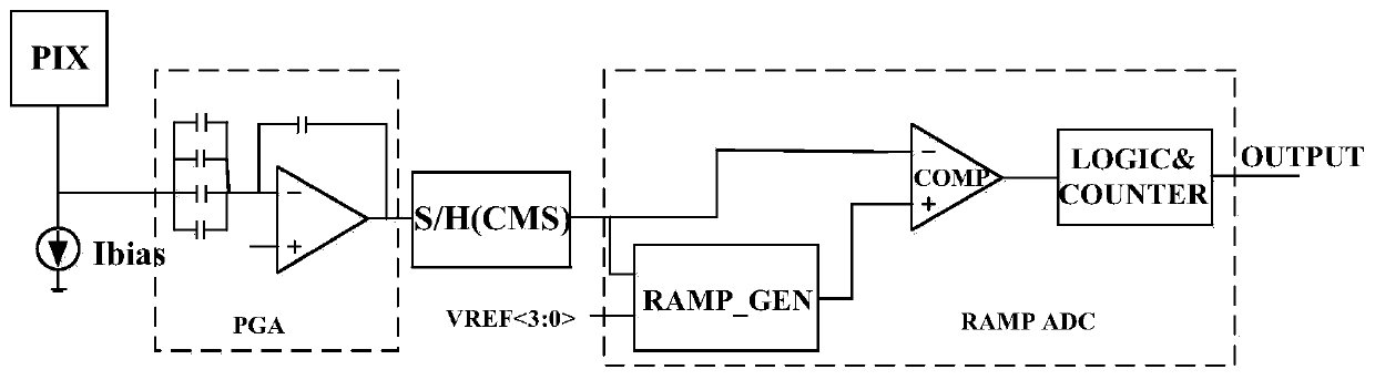
[0023] The image sensor described in the present invention is completely compatible with standard CMOS technology. The following describes the readout process of an image sensor in detail based on the 0.18 μm standard CMOS technology with reference to the accompanying drawings and examples.

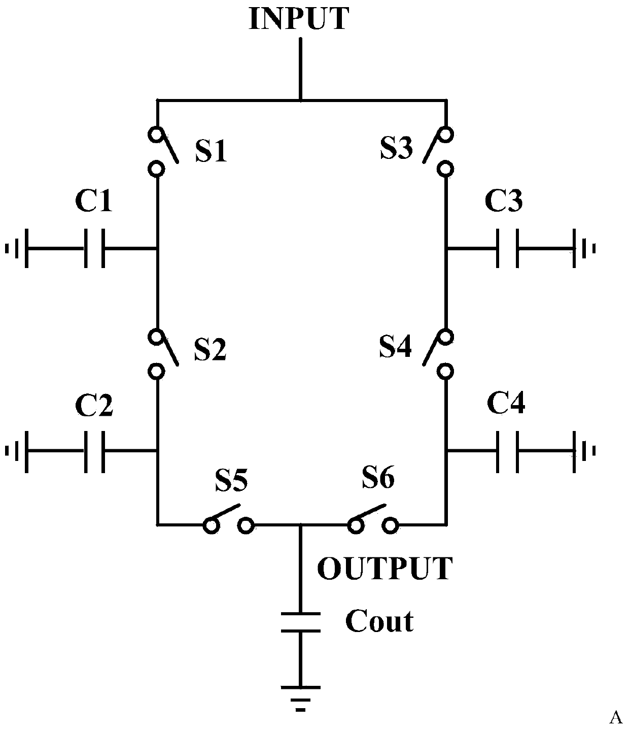
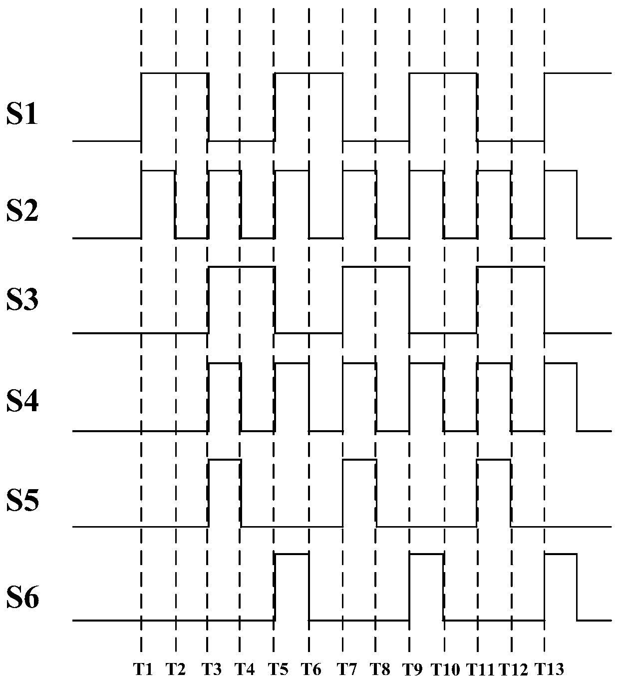
[0024] like figure 1 Shown, an ultra-low noise image sensor readout circuit based on CMS, including active pixels, column bus current source, gain programmable amplifier, sample and hold circuit with CMS function and ramp ADC with CMS function (Analog-to-digital converter, analog-to-digital converter); wherein, the light from the scene is focused on each pixel through the optical system, and the light intensity information is converted into a voltage signal through the active pixel, and the voltage signal is transmitted through the column bus. To the input of the gain-programmable amplifier, the column bus current source provides bias current for the pixel's internal source follower and ...


PUM


Abstract

The invention discloses a low-noise image sensor reading circuit architecture based on a CMS technology and belongs to the technical field of semiconductor image sensing. The reading circuit comprisesa front-end active pixel, a gain programmable amplifier, a sampling hold circuit with a correlation multiple sampling function and a low-power-consumption slope ADC with a correlation multiple sampling function. The CMS technology is applied to an analog part and a digital part at the same time in the same reading circuit, such that noise of the reading circuit is effectively reduced, the standard of an ultra-low noise image sensor can be achieved, circuit advantages can be achieved according to specific application, and high compatibility is achieved. Meanwhile, the layout area and complexity of the circuit are greatly reduced, and the utilization rate of the chip area is higher.

Description

technical field [0001] The invention belongs to the technical field of semiconductor image sensing, and in particular relates to a readout circuit of a CMOS image sensor based on CMS (Correlated Multiple Sampling) technology. Background technique [0002] CMOS image sensors are now widely used in people's work and life because of their high integration and low cost. Over the years, the technology and performance of CMOS sensors have advanced by leaps and bounds, and they are not only limited to some low-end consumer and monitoring. They can also be often seen in some high-end scientific, biological imaging, industrial, aerospace and other applications. Most high-end applications require CMOS sensors with high dynamic range, high speed, low noise, low dark current, and global shutter. [0003] Noise is one of the important indicators to measure the quality of image sensors, so the research on noise of analog readout circuits of image sensors is also a hot spot. The commonly...

Claims


Application Information

Patent Timeline
Patent Type & Authority Applications(China)
IPC IPC(8): H04N5/374H04N5/378H04N5/357
CPCH04N25/60H04N25/76H04N25/75H04N25/616H04N25/618
Inventor 殷景志刘芳园常玉春
Owner 长光(沧州)光栅传感技术有限公司
Features
  • R&D
  • Intellectual Property
  • Life Sciences
  • Materials
  • Tech Scout
  • Unparalleled Data Quality
  • Higher Quality Content
  • 60% Fewer Hallucinations
Learn More