

Heat dissipation type single/double-fiber pluggable optical module, and assembling method and outer clamping fastener thereof
A heat-dissipating, optical module technology, applied in optical components, light guides, optics, etc., can solve problems such as damage to the internal chip components of the optical module, performance degradation, and disability of the optical module, and achieve the effect of excellent external heat conduction effect.
- Summary
- Abstract
- Description
- Claims
- Application Information
AI Technical Summary
Problems solved by technology
Method used
Image

Examples
Embodiment Construction
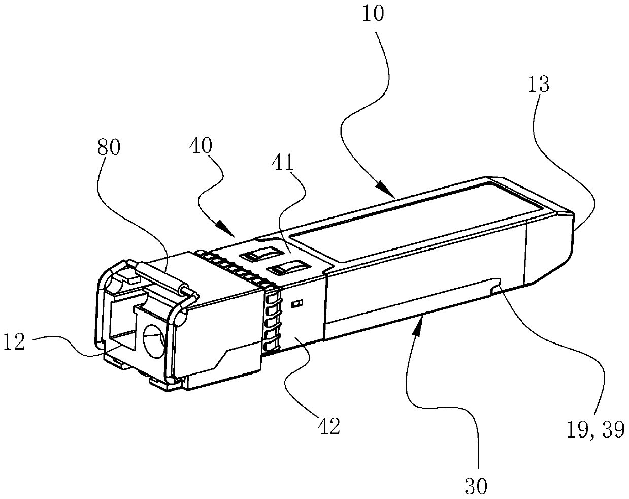
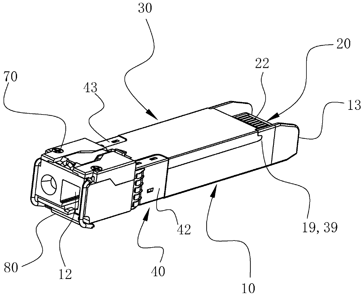
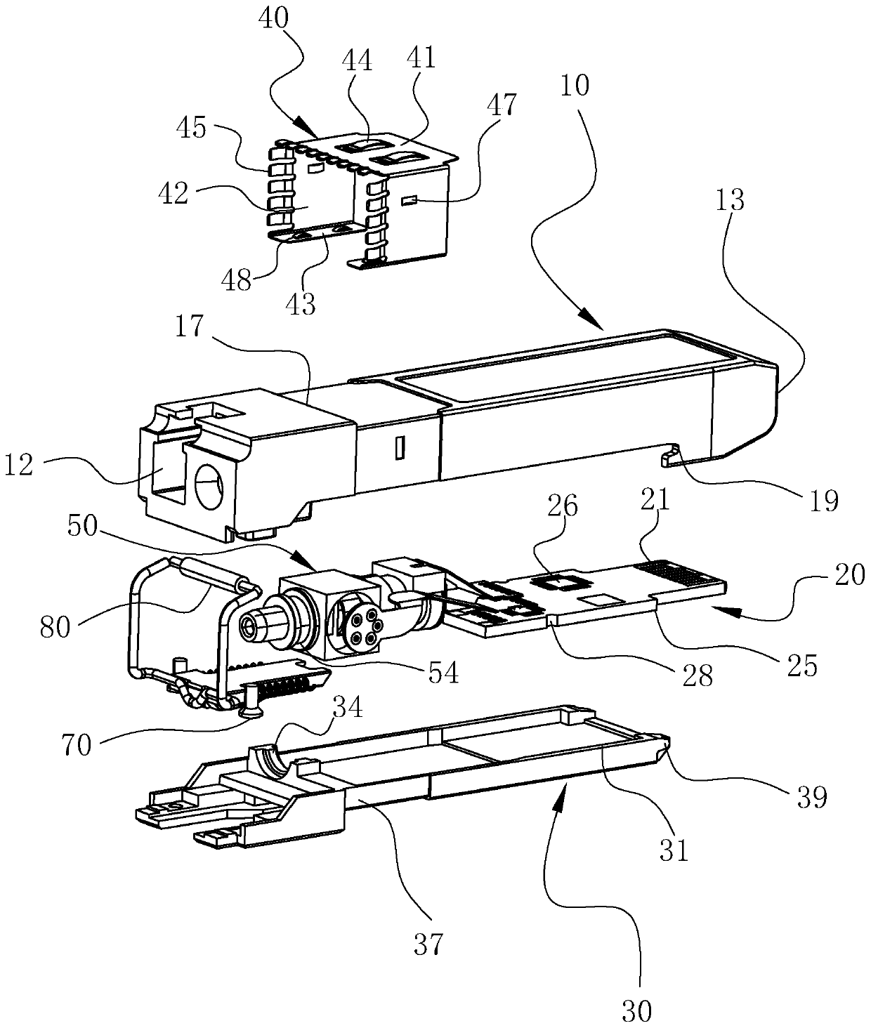
[0062] The technical solutions in the embodiments of the present invention will be clearly and completely described below in conjunction with the accompanying drawings in the embodiments of the present invention. Apparently, the described embodiments are only part of the embodiments for understanding the inventive concepts of the present invention, and cannot represent All the embodiments are not explained as the only embodiment. Based on the embodiments of the present invention, all other embodiments obtained by persons of ordinary skill in the art on the premise of understanding the inventive concepts of the present invention fall within the protection scope of the present invention.
[0063] It should be noted that if there is a directional indication (such as up, down, left, right, front, back...) in the embodiment of the present invention, the directional indication is only used to explain the position in a certain posture (as shown in the accompanying drawing). If the sp...
PUM
 Abstract
Description
Claims
Application Information