
Mask plate and manufacturing method thereof

A manufacturing method and mask technology, applied in ion implantation plating, metal material coating process, coating, etc., can solve the problems of influence, fine metal mask hole size and hole distance limitation, etc., to reduce brightness Effects of unevenness, improvement of picture quality, and reduction of stress unevenness

Inactive Publication Date: 2020-06-05
INCOFLEX SEMICON TECH CO LTD
View PDF6 Cites 0 Cited by
  • Summary
  • Abstract
  • Description
  • Claims
  • Application Information

AI Technical Summary

Problems solved by technology

This process limits the hole size and pitch of the fine metal mask, which in turn affects the evaporation of high pixel density (Pixels Per Inch, PPI) displays.

Method used


Image

  • Mask plate and manufacturing method thereof
  • Mask plate and manufacturing method thereof
  • Mask plate and manufacturing method thereof

Examples


Embodiment Construction

[0031] Example embodiments will now be described more fully with reference to the accompanying drawings. Example embodiments may, however, be embodied in many forms and should not be construed as limited to the examples set forth herein; rather, these embodiments are provided so that this disclosure will be thorough and complete and will fully convey the concept of example embodiments to those skilled in the art. The described features, structures, or characteristics may be combined in any suitable manner in one or more embodiments.

[0032] Furthermore, the drawings are merely schematic illustrations of the present disclosure and are not necessarily drawn to scale. The same reference numerals in the drawings denote the same or similar parts, and thus repeated descriptions thereof will be omitted. Some of the block diagrams shown in the drawings are functional entities and do not necessarily correspond to physically or logically separate entities.

[0033] In this exemplary...


PUM


Abstract

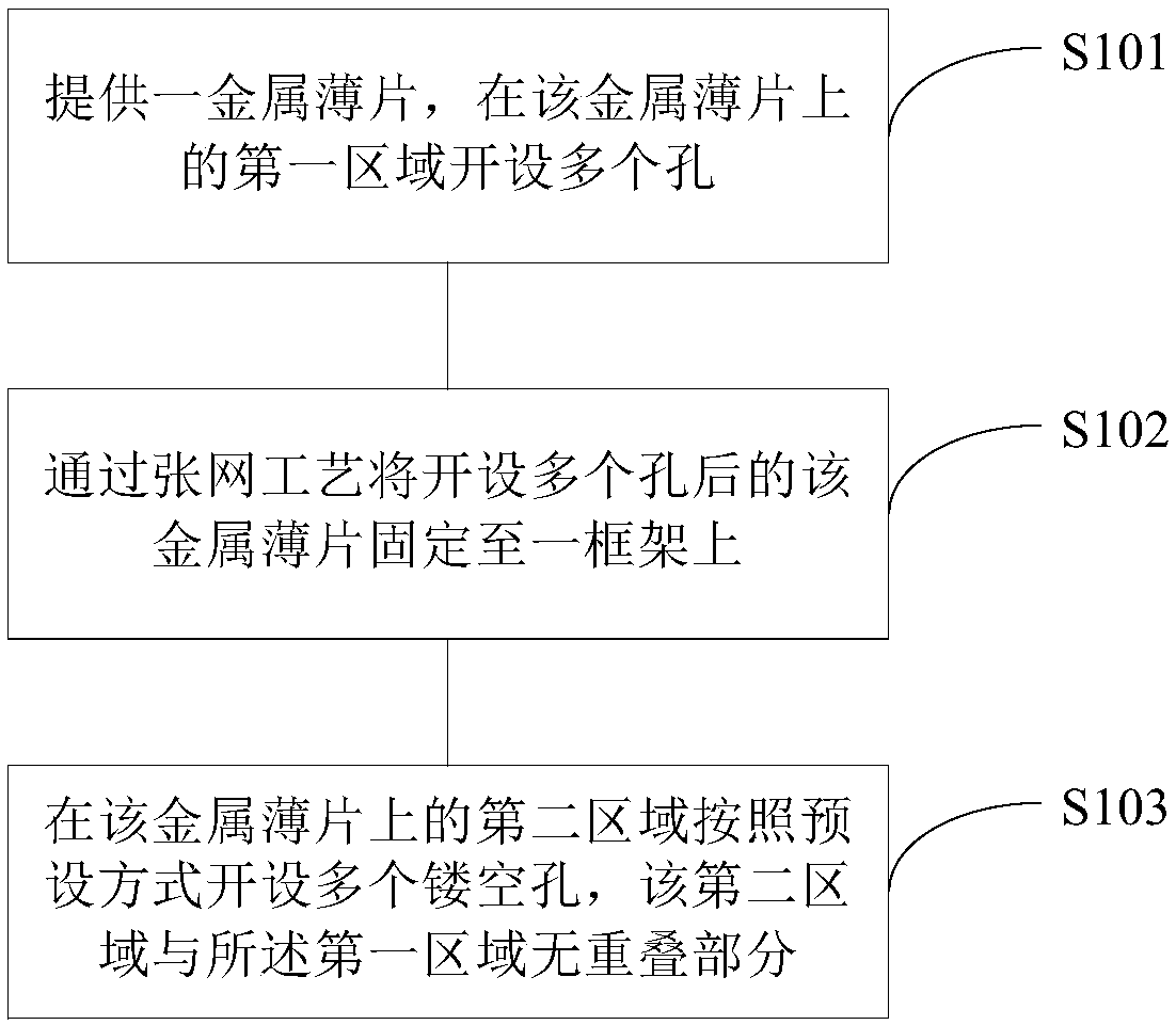
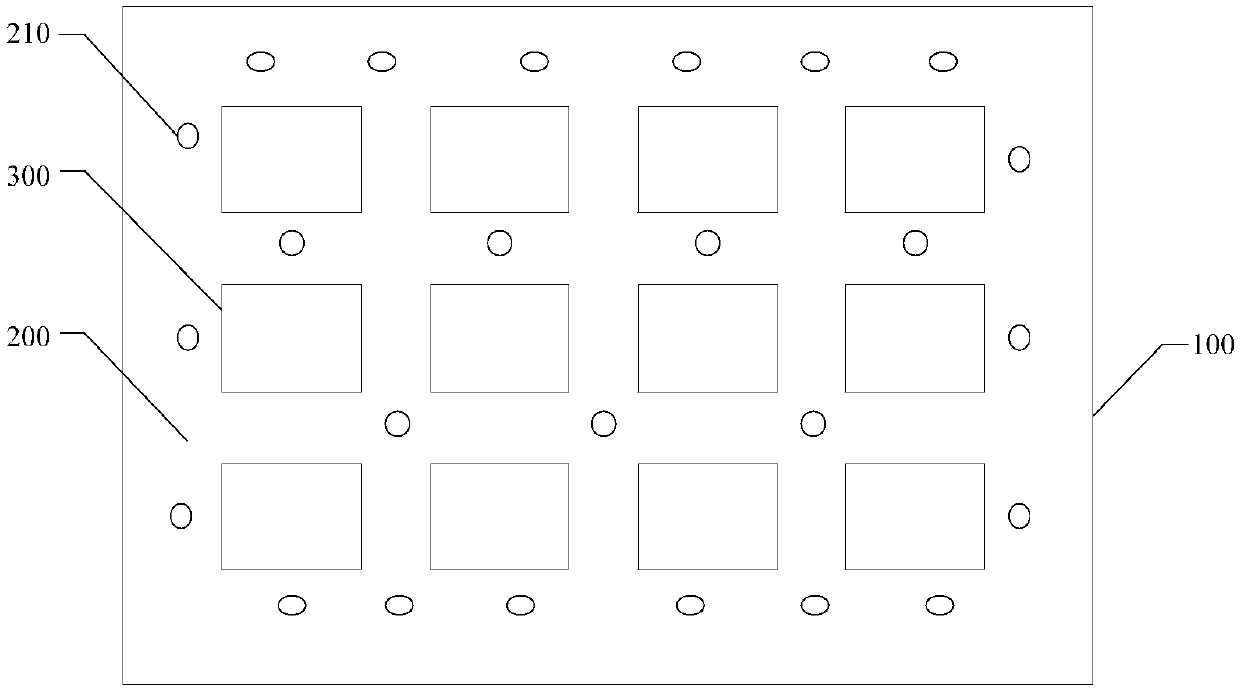
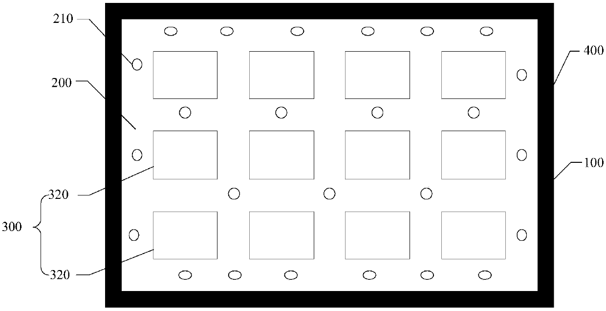
The invention relates to a mask plate and a manufacturing method thereof. The manufacturing method of the mask plate includes the steps that a metal sheet is provided, and multiple holes are formed ina first area on the metal sheet; the metal sheet with the multiple holes formed is fixed to a frame through a net stretching process; and multiple hollow-out holes are formed in a second area on themetal sheet in a preset mode, and the second area and the first area are not overlapped. The mask plate manufactured through the disclosed manufacturing method is beneficial to evaporation of a high-PPI displayer, the phenomenon that the brightness of devices such as an AMOLED is uneven is eliminated, and the image quality of the devices such as the AMOLED is improved to a certain degree.

Description

technical field [0001] The invention relates to the field of display technology, in particular to a mask plate and a manufacturing method thereof. Background technique [0002] Display technology is a technology that uses electronic technology to provide flexible visual information. With the development of display technology, people's demand for display quality is increasing, and high-quality, high-resolution display devices are increasingly popular among display panel manufacturers. attention. Active Matrix Organic Light Emitting Diode (AMOLED) originates from Organic Light Emitting Diode (OLED) technology, and has characteristics such as self-luminescence, low power consumption, and fast response. In the manufacturing process of AMOLED devices, high-vacuum evaporation is usually used to manufacture the organic layer of the device, and the evaporation process requires a fine metal mask (Fine Metal Mask, FMM) to define the position of the coating. [0003] In the related a...

Claims


Application Information

Patent Timeline
Patent Type & Authority Applications(China)
IPC IPC(8): C23C14/04C23C14/24C23C14/12
CPCC23C14/042C23C14/12C23C14/24
Inventor 陈秉宏
Owner INCOFLEX SEMICON TECH CO LTD
Learn More