Preparation method of in-situ electrical TEM sample

A sample, in-situ technology, applied in the field of TEM sample preparation, can solve the problem of inability to directly observe the continuous change of the microstructure of the material, and achieve the effect of high universality and simple process

Active Publication Date: 2020-06-05
TIANJIN UNIVERSITY OF TECHNOLOGY
View PDF8 Cites 3 Cited by
  • Summary
  • Abstract
  • Description
  • Claims
  • Application Information

AI Technical Summary

Problems solved by technology

[0004]The purpose of the present invention is to overcome the shortcoming that the continuous change of the material microstructure and performance cannot be directly observed in the current ex-situ ...

Method used


Image

  • Preparation method of in-situ electrical TEM sample
  • Preparation method of in-situ electrical TEM sample
  • Preparation method of in-situ electrical TEM sample

Examples


Embodiment 1

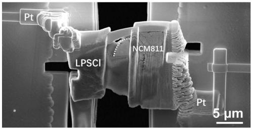
[0023] Preparation of NCM811 / LPSCl in situ electrical TEM samples

[0024] (1) Connect the solid-state electrolyte and the electrode material using the magnetron sputtering method.

[0025] Put the electrode material NCM811 and the solid electrolyte target LPSCl into the magnetron sputtering furnace, sputter for about 50 minutes under the condition of a pressure of 2Pa and a power of 100W, and cover the electrode material with a solid electrolyte of 800nm ​​to obtain an electrode / electrolyte Material.

[0026] (2) Put the electrode / electrolyte material prepared in step (1) into a focused ion beam electron microscope for processing.

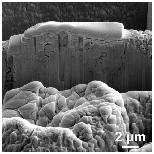
[0027] Adjust the height of the sample area to the height of the confocal, extend the Pt needle after preheating, deposit a Pt protective layer with a thickness of 800nm ​​with an ion beam of 30kV, 0.8nA, and control the beam current of FIB (Focused Ion Beam abbreviation, focused ion beam) at 26pA / um 2 . Choose 30kV, 6.5nA FIB beam to etch bot...

Embodiment 2

[0029] Preparation of Si / LiFePO 4 / LAGP in situ electrical TEM samples

[0030] (1) Connect the solid-state electrolyte and the electrode material using the magnetron sputtering method.

[0031] Si substrate and LiFePO 4 Put it into a magnetron sputtering furnace, and sputter the ceramic composite electrolyte (LAGP) for 20 minutes under the conditions of a pressure of 2Pa and a power of 60W to obtain a 100nm LAGP. Thus an electrode / electrolyte material is obtained.

[0032](2) Put the electrode / electrolyte material prepared in step (1) into a focused ion beam electron microscope for processing.

[0033] Adjust the height of the sample area to the height of the confocal, extend the Pt needle after preheating, deposit a Pt protective layer with a thickness of 1um with an ion beam of 30kV, 0.8nA, and control the beam current of the FIB at 26pA / um 2 . Choose 30kV, 6.5nA FIB beam to etch both sides of the TEM sheet, the termination position is the edge of the Pt protective lay...


PUM


Abstract

The invention discloses a preparation method of an in-situ electrical TEM sample. The method comprises the following steps: connecting an electrode material and a solid electrolyte by using a magnetron sputtering method, then placing the electrode/electrolyte material in a focused ion beam-electron beam double-beam electron microscope, depositing a protective layer on the surface, etching, cuttingoff and extracting a TEM sheet. A circulating electrode of the in-situ heating chip, the in-situ heating chip is refitted into a double-electrode power-up chip, the double-electrode power-up chip isconnected with the TEM sheet, the double-electrode power-up chip is bidirectionally shearing until the thickness is about 200nm, and an amorphous layer is removed until the thickness of the amorphouslayer is below 100nm to obtain thein-situ electrical TEM sample. According to the invention, scanning electron microscopy is combined with in-situ transmission electron microscopy,and dynamic observation of charge distribution of an electrode/electrolyte interface or an electrode internal interface on working conditions and a microcosmic scale is achieved. The preparation process is simple, and the universality is high.

Description

technical field [0001] The invention relates to a transmission electron microscope (TEM) sample, in particular to a method for preparing a TEM sample that can study material structure and property changes in an in-situ electrified environment. Background technique [0002] Most of the TEM characterizations are static, and thus the stable structure of the material in an equilibrium state is obtained, which is also called ex-situ characterization. It is usually difficult to capture and characterize the structural evolution of materials under working conditions ex situ, which hinders the construction of their true structure-activity relationship, and it is also difficult to optimize materials from the perspective of structural degradation. The semi-in-situ electron microscopic characterization has taken another step forward in the research on the relationship between the structure and properties of materials. After the material has completed the reaction outside the electron mi...

Claims


Application Information

Patent Timeline
IPC IPC(8): G01N1/28G01N23/22
CPCG01N1/28G01N23/22Y02E60/10
Inventor 周峒李超罗俊
Owner TIANJIN UNIVERSITY OF TECHNOLOGY
Why Eureka
Try Eureka