Reworking method of bonding pad crystallization defects and semiconductor device

A crystal defect, semiconductor technology, applied in the direction of semiconductor devices, semiconductor/solid-state device manufacturing, semiconductor/solid-state device components, etc., can solve the problems of pad crystalline defects, pad surface crystalline defects, etc., to reduce scrap, beneficial to The effect of process cost control

Pending Publication Date: 2020-06-12
WUHAN XINXIN SEMICON MFG CO LTD
View PDF9 Cites 0 Cited by
  • Summary
  • Abstract
  • Description
  • Claims
  • Application Information

AI Technical Summary

Problems solved by technology

[0005] The object of the present invention is to provide a method for reworking crystallization defects of pads and a semiconductor device to solve the problem of crystallization defects on the surface of pads

Method used


Image

  • Reworking method of bonding pad crystallization defects and semiconductor device
  • Reworking method of bonding pad crystallization defects and semiconductor device
  • Reworking method of bonding pad crystallization defects and semiconductor device

Examples


Embodiment Construction

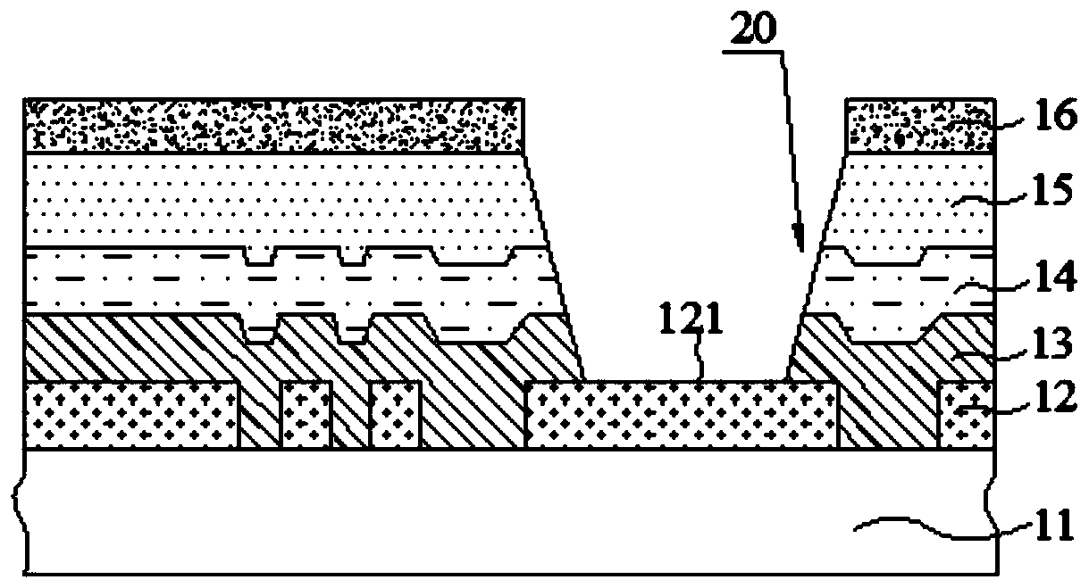
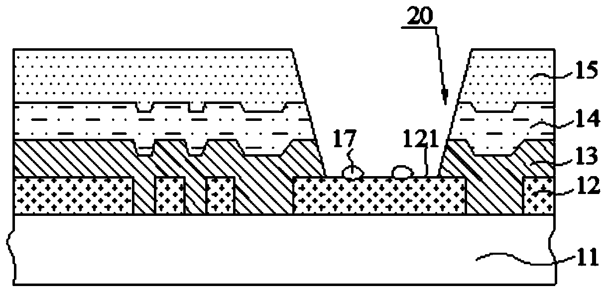
[0035] Based on the above studies, embodiments of the present invention provide a method for reworking crystallization defects of bonding pads and a semiconductor device. The present invention will be described in further detail below in conjunction with the accompanying drawings and specific embodiments. The advantages and features of the present invention will become clearer from the following description. It should be noted that the drawings are all in a very simplified form and use imprecise scales, and are only used to facilitate and clearly assist the purpose of illustrating the embodiments of the present invention.

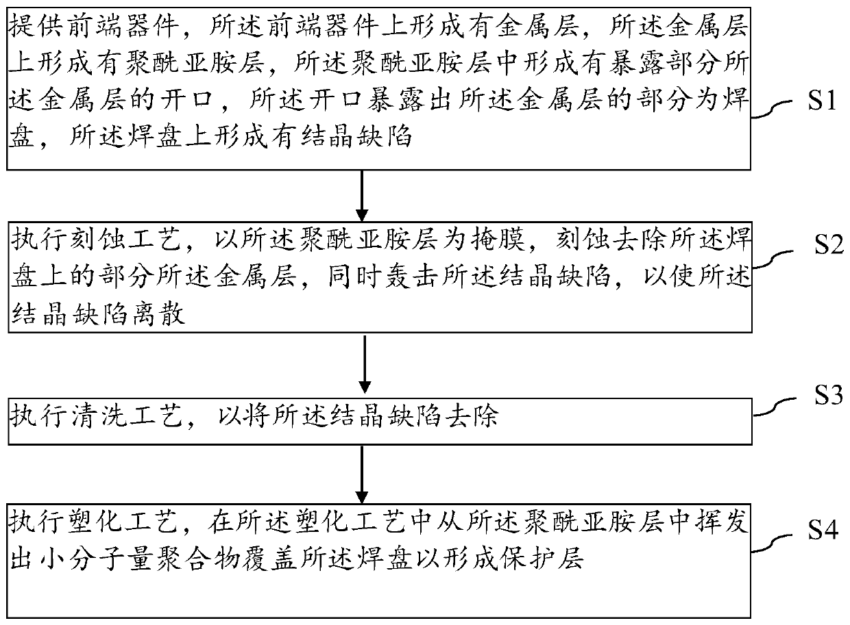
[0036] An embodiment of the present invention provides a rework method for pad crystal defects, such as figure 1 shown, including:

[0037] A front-end device is provided, a metal layer is formed on the front-end device, a polyimide layer is formed on the metal layer, an opening exposing part of the metal layer is formed in the polyimide layer, and the op...


PUM

PropertyMeasurementUnit
thicknessaaaaaaaaaa
thicknessaaaaaaaaaa

Abstract

The invention provides a reworking method of bonding pad crystallization defects and a semiconductor device, and the method comprises the steps: providing a front-end device, forming a metal layer onthe front-end device, forming a polyimide layer on the metal layer, and forming a crystallization defect on a bonding pad; taking the polyimide layer as a mask, etching to remove part of the metal layer on the bonding pad, bombarding the crystallization defect to disperse the crystallization defect, and enabling the polyimide layer to play roles of the mask layer and the passivation layer; then carrying out a cleaning process to remove crystallization defects; and performing a plasticizing process to form a protective layer covering the bonding pad, the protective layer not only blocking the generation of crystal defects, but also preventing the generated crystal defects from eroding the reworked wafer. According to the invention, the problem of crystallization defects on the surface of the bonding pad of the semiconductor device taking polyimide as the passivation layer can be effectively solved, and scrap is reduced through reworking. The process of forming a patterned mask layer onthe passivation layer in a conventional rework process is omitted, and process cost control is facilitated.

Description

technical field [0001] The invention belongs to the technical field of integrated circuit manufacturing, and in particular relates to a rework method for pad crystal defects and a semiconductor device. Background technique [0002] In the manufacturing process of semiconductor devices, after the device structure and interconnection structure are formed on the wafer, a passivation layer will be formed on the wafer to protect the internal devices. The passivation layer has openings that expose the pads. In practical applications, it is found that crystallization defects are easily formed on the surface of the pads. The back-end process of semiconductor device (wafer) manufacturing is often affected by the crystallization defects of the pads. The usual rework method is to form a patterned mask layer (such as a patterned photoresist layer) on the passivation layer of the semiconductor device (wafer), and use the patterned mask layer as a mask to etch and remove Pad crystallizat...

Claims


Application Information

Patent Timeline
Patent Type & Authority Applications(China)
IPC IPC(8): H01L21/3065H01L21/02H01L23/488
CPCH01L21/3065H01L21/02057H01L23/488
Inventor 李乔伟胡胜赵长林
Owner WUHAN XINXIN SEMICON MFG CO LTD
Why Eureka
Try Eureka