Trench gate power MOSFET and manufacturing method thereof

A manufacturing method and trench gate technology, which is applied in semiconductor/solid-state device manufacturing, electrical components, circuits, etc., can solve the problems of high manufacturing cost of power devices and difficult process control, so as to reduce the injection energy and make the manufacturing process easy to control , Reduce the effect of parasitic capacitance

Inactive Publication Date: 2020-06-12
INVENTCHIP TECH CO LTD
View PDF2 Cites 4 Cited by
  • Summary
  • Abstract
  • Description
  • Claims
  • Application Information

AI Technical Summary

Problems solved by technology

However, the manufacturing cost of power devices with trench gate and super junction structure is high, and the process control is difficult

Method used


Image

  • Trench gate power MOSFET and manufacturing method thereof
  • Trench gate power MOSFET and manufacturing method thereof
  • Trench gate power MOSFET and manufacturing method thereof

Examples


Embodiment Construction

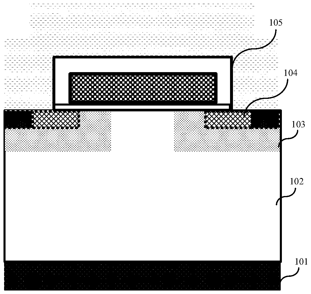
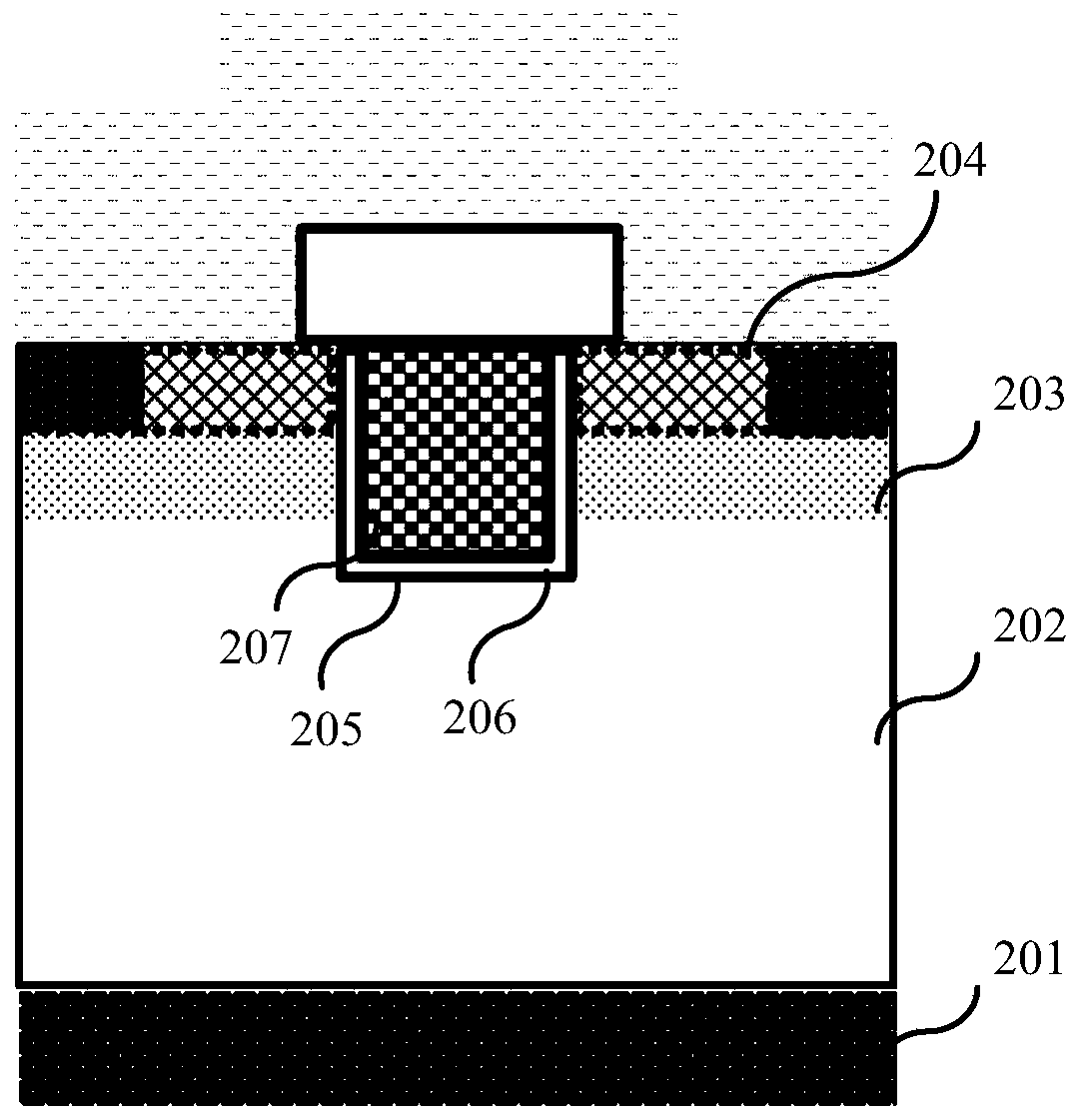
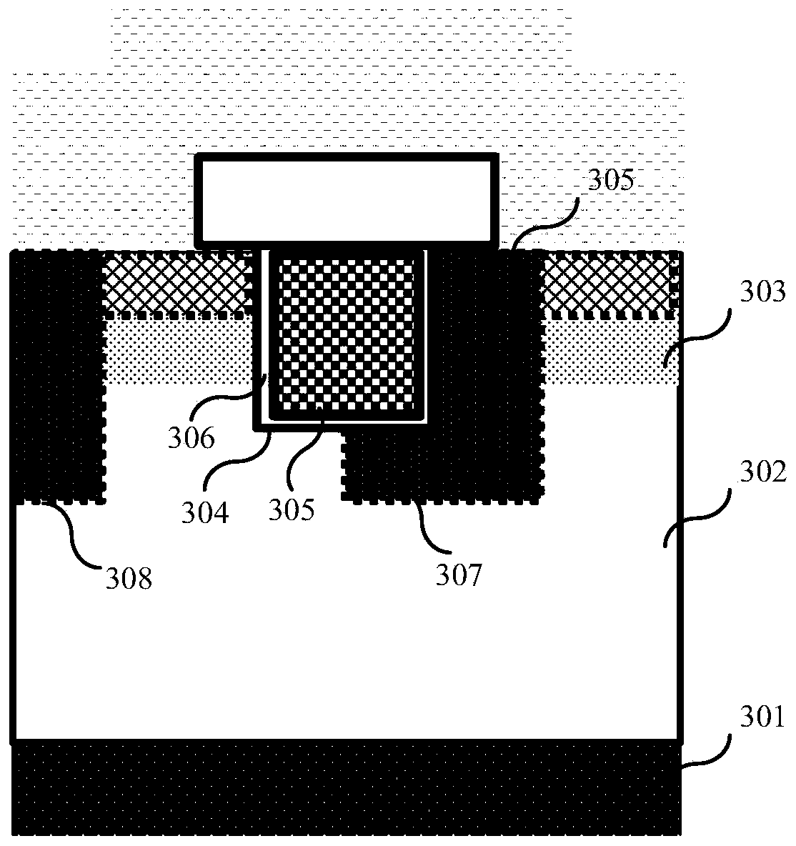
[0046] Illustrative embodiments of the present application include, but are not limited to, trench gate power MOSFETs and methods of fabrication thereof.

[0047]Reference will now be made in detail to the exemplary embodiments, examples of which are illustrated in the accompanying drawings. When the following description refers to the accompanying drawings, the same numerals in different drawings refer to the same or similar elements unless otherwise indicated. The implementations described in the following exemplary embodiments do not represent all implementations consistent with this application. Rather, they are merely examples of apparatuses and methods consistent with aspects of the present application as recited in the appended claims.

[0048] The terminology used in this application is for the purpose of describing particular embodiments only, and is not intended to limit the application. As used in this application and the appended claims, the singular forms "a", "...


PUM

PropertyMeasurementUnit
thicknessaaaaaaaaaa
thicknessaaaaaaaaaa

Abstract

The invention relates to the field of semiconductors, and discloses a trench gate power MOSFET and a manufacturing method thereof. The manufacturing method of the trench gate power MOSFET comprises the following steps: growing an epitaxial layer with a first conductivity type on a wide bandgap semiconductor substrate; forming a body region with a second conductivity type on the epitaxial layer; forming a groove in the body region through etching; implanting first ions into the bottom region of the trench along the crystal orientation of the wide bandgap semiconductor material, forming a secondconductive type column, the bottom region of the trench being located below the trench and being connected with the bottom of the trench, the selection of the crystal orientation being such that theimplantation of the first ions can utilize a crystal channel effect, and the longitudinal depth of the second conductive type column being at least not less than 50% of the thickness of the epitaxiallayer located at the bottom region of the trench; and filling filler into the groove to fill the groove.

Description

technical field [0001] The present application relates to the field of semiconductors, in particular to a trench gate power MOSFET and a manufacturing method thereof. Background technique [0002] Semiconductor devices such as power MOSFETs have been widely used in automotive electronics, switching power supplies, and industrial control. In order to continuously improve power conversion efficiency and power density, it is very important to design high-efficiency power switching devices such as power MOSFETs. The most important performance parameter of a power MOSFET is the characteristic on-resistance Rsp, and the on-resistance between the drain and the source is proportional to the power consumed by the power MOSFET device. Under the same breakdown voltage, for devices with the same on-resistance, the smaller the characteristic on-resistance, the smaller the chip area and the lower the parasitic capacitance of the power MOSFET, thus reducing the switching of the power MOSF...

Claims


Application Information

Patent Timeline
Patent Type & Authority Applications(China)
IPC IPC(8): H01L29/78H01L29/423H01L29/16H01L21/04
CPCH01L29/78H01L29/4236H01L29/1608H01L29/66068H01L29/7813
Inventor 张永熙陈伟黄海涛
Owner INVENTCHIP TECH CO LTD
Why Eureka
Try Eureka