Carbon nanotube/graphene van der Waals heterojunction photoelectric device, its construction method and application

A carbon nanotube and optoelectronic device technology, which is applied in the field of carbon nanotube/graphene van der Waals heterojunction optoelectronic devices, can solve the problems of limiting the detectability of the device, large dark current of the device, etc., achieves high-efficiency charge transfer efficiency, improves optoelectronic performance, the effect of reducing the chance of recombination

Active Publication Date: 2020-09-25
南京晶碳纳米科技有限公司 +1
View PDF3 Cites 0 Cited by
  • Summary
  • Abstract
  • Description
  • Claims
  • Application Information

AI Technical Summary

Problems solved by technology

However, the ultra-high conductivity of graphene makes the dark current of the device larger, which limits the improvement of the detectable rate of the device.

Method used


Image

  • Carbon nanotube/graphene van der Waals heterojunction photoelectric device, its construction method and application
  • Carbon nanotube/graphene van der Waals heterojunction photoelectric device, its construction method and application
  • Carbon nanotube/graphene van der Waals heterojunction photoelectric device, its construction method and application

Examples


Embodiment 1

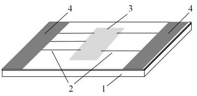
[0030] This embodiment provides a carbon nanotube / graphene van der Waals heterojunction optoelectronic device and its preparation method, its structural schematic diagram is as follows figure 2 shown. Its construction method is as follows:

[0031] (1) Si / SiO 2 The substrate is used as an insulating base, in Si / SiO 2 CVD grown graphene was transferred on the substrate by wet transfer method.

[0032] (2) The photolithography process is used to etch the inter-electrodes into a graphene pattern structure, and the excess graphene is removed by an oxygen plasma etching process.

[0033] (3) Leave grooves at the position where the carbon nanotubes need to be aligned by photolithography. The density of permanent carbon nanotubes is 100 / μm; the carbon tubes except the grooves are cleaned by the lift-off process.

[0034] (4) The pattern of the electrode is photoetched through the photolithography process, and the patterned Au electrode pair is deposited by the traditional micro...

Embodiment 2

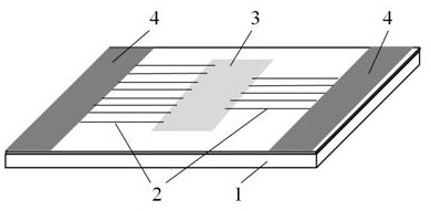
[0037] This embodiment provides a carbon nanotube / graphene van der Waals heterojunction optoelectronic device and its preparation method, its structural schematic diagram is as follows image 3 shown. Its construction method is as follows:

[0038] (1) Si / SiO 2 The substrate is used as an insulating base, in Si / SiO 2 CVD grown graphene was transferred on the substrate by wet transfer method.

[0039] (2) The photolithography process is used to etch the structure of two graphene patterns between the electrodes, and the excess graphene is removed by an oxygen plasma etching process.

[0040] (3) Leave grooves at the position where the carbon nanotubes need to be aligned by photolithography. The density of permanent carbon nanotubes is 20 / μm; the carbon tubes except the grooves are cleaned by the lift-off process.

[0041] (4) The pattern of the electrode is photoetched through the photolithography process, and the patterned Au electrode pair is deposited by the traditional ...

Embodiment 3

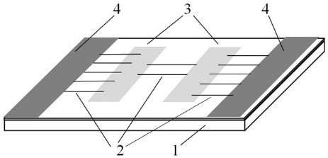
[0044] This embodiment provides a carbon nanotube / graphene van der Waals heterojunction optoelectronic device and its preparation method, its structural schematic diagram is as follows Figure 4 shown. Its construction method is as follows:

[0045] (1) Si / SiO 2 The substrate is used as an insulating base, in Si / SiO 2 CVD grown graphene was transferred on the substrate by wet transfer method.

[0046] (2) The photolithography process is used to etch the structure of four graphene patterns between the electrodes, and the excess graphene is removed by an oxygen plasma etching process.

[0047] (3) Leave grooves at the position where the carbon nanotubes need to be aligned by photolithography. The groove spacing is 5 μm. The semiconductor single-walled carbon nanotubes are transferred to the sample by AC dielectrophoresis, and the graphene space is patterned. The density of the aligned semiconducting carbon nanotubes is 1 / μm; the carbon tubes except the grooves are cleaned by t...


PUM


Abstract

The invention discloses a carbon nanotube / graphene van der Waals heterojunction optoelectronic device, a construction method and application thereof, and belongs to the technical field of semiconductor optoelectronic devices. Including: an insulating substrate, electrode pairs arranged on both sides of the upper surface of the insulating substrate, patterned graphene between the electrode pairs, semiconducting carbon nanotubes with directional arrangement and controllable density between the patterned graphenes . Compared with the prior art, the present invention adopts patterned graphene and directionally arranged semiconducting carbon nanotubes to form a van der Waals heterostructure, and can make full use of the ultra-high carrier mobility and high carrier mobility of graphene and semiconducting carbon nanotubes. Light-absorbing capacity of semiconducting carbon nanotubes. More importantly, by adjusting the arrangement density of semiconducting carbon nanotubes and the size of patterned graphene, the photoresponsivity of the device can be increased while the dark current of the device can be greatly reduced, thereby improving the specific detectivity of the device.

Description

technical field [0001] The invention belongs to the technical field of semiconductor photoelectric devices, in particular to a carbon nanotube / graphene van der Waals heterojunction photoelectric device, its construction method and application. Background technique [0002] The excellent electrical, thermal, mechanical properties, chemical stability and unique one-dimensional nanostructure of carbon nanotubes (CNTs) make them ideal functional materials for use in micro-nano electronic devices. In particular, semiconducting half-walled carbon nanotubes (SWCNTs) have good light absorption in the entire spectral region from UV-vis-NIR (especially in the near-infrared region), and their light absorption coefficient (10 4 -10 5 cm -1 ) is 1-2 orders of magnitude higher than traditional semiconductor materials, and has femtosecond response characteristics to light. Therefore, optoelectronic devices based on semiconducting SWCNTs are expected to achieve extremely high photoelectr...

Claims


Application Information

Patent Timeline
Patent Type & Authority Patents(China)
IPC IPC(8): H01L31/028H01L31/074H01L31/18
CPCH01L31/028H01L31/074H01L31/1804Y02E10/547Y02P70/50
Inventor 苏言杰叶小亮俞健
Owner 南京晶碳纳米科技有限公司
Why Eureka
Try Eureka