High-resolution spectrograph based on etched diffraction grating

An etching diffraction grating, high-resolution technology, applied in the field of high-resolution spectrometers, can solve the problems of affecting resolution, output channel crosstalk, device resolution difficulties, etc., and achieve the effect of high resolution and low crosstalk

Pending Publication Date: 2020-06-23
绍兴图聚光电科技有限公司
View PDF4 Cites 1 Cited by
  • Summary
  • Abstract
  • Description
  • Claims
  • Application Information

AI Technical Summary

Problems solved by technology

[0003] In the prior art, the on-chip spectrometer generally adopts the traditional equal-width array waveguide as the output waveguide. The width of each output channel of the output waveguide is the same, and the distance between adjacent output channels can reach 2.5um. When the distance continues to be reduced, the distance between the output channels The crosstalk phenomenon between them affects the resolution
When the spacing between the output channels is smaller, the resolution of the on-chip spectrometer is higher, and the spacing requirements of equal-width output channels make it more difficult to improve the resolution of the device

Method used


Image

  • High-resolution spectrograph based on etched diffraction grating
  • High-resolution spectrograph based on etched diffraction grating
  • High-resolution spectrograph based on etched diffraction grating

Examples


Embodiment

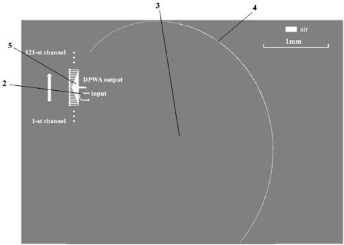
[0033] Such as figure 1 and figure 2 As shown, a high-resolution spectrometer based on an etched diffraction grating includes a substrate 1 , an input waveguide 2 , a free transmission region 3 , a reflective grating 4 and an output waveguide 5 . The input waveguide 2 , the free transmission area 3 , the reflective grating 4 and the output waveguide 5 are integrated on the substrate 1 . In this embodiment, the substrate 1 is an SOI substrate, and the thickness of the substrate is preferably 220nm. The input waveguide 2, reflection grating 3 and output waveguide 5 are prepared on the substrate by photolithography, and the rest of the area is the free transmission area 3.

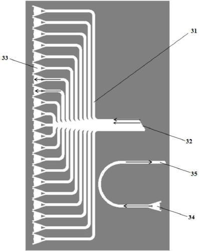
[0034] image 3 It is a partial enlarged view of the input waveguide and output waveguide of a preferred embodiment of the high-resolution spectrometer based on an etched diffraction grating in the present invention. The input and output adopt grating coupling. As shown in the figure, the output waveguide ...


PUM

PropertyMeasurementUnit
thicknessaaaaaaaaaa

Abstract

The invention provides a high-resolution spectrograph based on an etched diffraction grating. The high-resolution spectrograph comprises a substrate, an input waveguide, a free transmission area, a reflection grating and an output waveguide which are integrated on the substrate, the input waveguide is used for receiving an optical signal to be measured and transmitting the optical signal to the free transmission area; the free transmission area transmits the light to be measured emitted from the input waveguide and the light to be measured reflected by the reflection grating; the reflection grating is used for reflecting the optical signal to be measured to the incident end of the output waveguide, so that the reflected light meets the condition of interference elongation at the incident end of the output waveguide; and the output waveguide is a dense array waveguide, the dense array waveguide is formed by circularly arranging a plurality of waveguides with different widths, each waveguide is an output channel, and each output channel outputs light with different wavelengths. Compared with a spectrometer using an equal-width array waveguide as an output waveguide, the spectrographhas the advantages that under the condition of the same spectrometer device size, the number of output channels is larger, the distance between the output channels is smaller, and the spectrometer resolution ratio is higher.

Description

technical field [0001] The invention belongs to the field of optical technology, and in particular relates to a high-resolution spectrometer based on an etched diffraction grating. Background technique [0002] Spectrometers are of great significance in chemical and biological sensing, material analysis, and light source characterization. High-resolution on-chip spectrometers provide low-cost and compact spectral analysis techniques for portable sensing. In recent years, silicon-on-insulator (SOI, Silicon-On-Insulator) integrated platform has attracted much attention due to its advantages of compactness, reliable performance, and high sensitivity, and has become an ideal platform for implementing on-chip spectrometers and on-chip laboratory systems. [0003] In the prior art, the on-chip spectrometer generally adopts the traditional equal-width array waveguide as the output waveguide. The width of each output channel of the output waveguide is the same, and the distance betw...

Claims


Application Information

Patent Timeline
Patent Type & Authority Applications(China)
IPC IPC(8): G01J3/18G01J3/28
CPCG01J3/1895G01J3/2823
Inventor 何赛灵马珂奇朱凝
Owner 绍兴图聚光电科技有限公司
Why Eureka
Try Eureka