
Manufacturing method of photomask with pattern

A manufacturing method and graphic technology, applied to the photoplate making process of patterned surface, optics, and originals for photomechanical processing, etc., which can solve the problems that the accuracy of photomask graphics needs to be improved.

Pending Publication Date: 2020-07-07
SEMICON MFG INT (SHANGHAI) CORP +1
View PDF6 Cites 2 Cited by
  • Summary
  • Abstract
  • Description
  • Claims
  • Application Information

AI Technical Summary

Problems solved by technology

[0004] However, the accuracy of the photomask pattern produced by the prior art needs to be improved

Method used


Image

  • Manufacturing method of photomask with pattern
  • Manufacturing method of photomask with pattern
  • Manufacturing method of photomask with pattern

Examples


Embodiment Construction

[0014] It can be seen from the background art that the accuracy of the photomask pattern produced by the prior art needs to be improved.

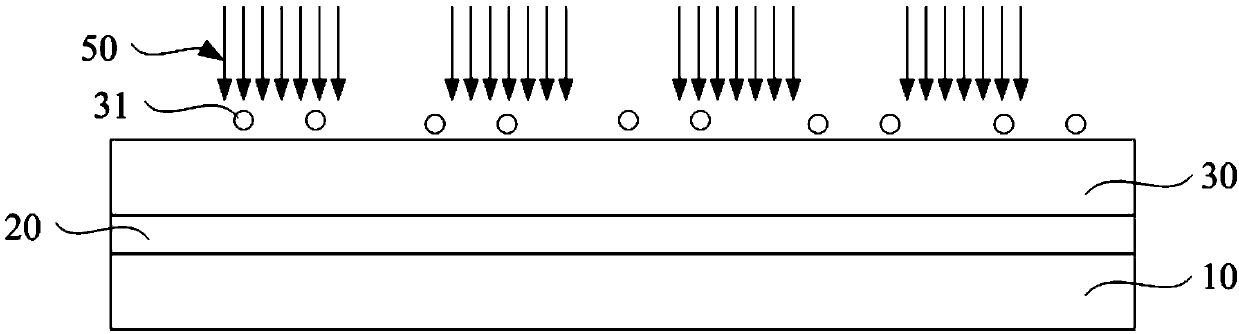
[0015] Now combined with a photomask manufacturing process for analysis, figure 1 and figure 2 It is a structural schematic diagram of a photomask manufacturing process, and the process steps of forming a photomask include: Refer to figure 1 , providing a carrier plate 10 and a mask plate 20 on the carrier plate 10; forming a photoresist layer 30 on the surface of the mask plate 20; transferring the design pattern to the In the photoresist layer 30 , exposure treatment is performed on the photoresist layer 30 .

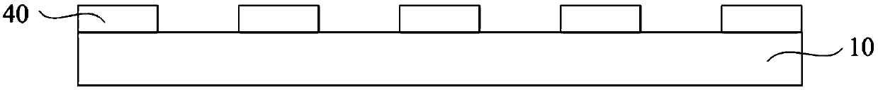
[0016] refer to figure 2 , to the photoresist layer 30 after the exposure treatment (refer to figure 1 ) for developing treatment, exposing part of the mask plate 20 (reference figure 1 ) surface; etching and removing the exposed mask plate 20 to form a patterned photomask 40; removing the photoresist layer 30.

[0017] The...


PUM


Abstract

The invention provides a manufacturing method of a photomask with a pattern. The manufacturing method comprises the steps of providing a design pattern and a standard test pattern; writing the standard test pattern by adopting a test electron beam lithography process, generating a test photomask, and obtaining a position deviation value between the test pattern and the standard test pattern in thetest photomask; writing the design pattern by adopting an actual electron beam lithography process; and generating a photomask with a pattern, and compensating the design pattern based on the obtained position deviation value in the actual electron beam lithography process so as to counteract the electron beam position deviation amount caused by reflected electrons in the actual electron beam lithography process to the position of the electron beam. According to the invention, the pattern position accuracy and the morphology accuracy in the photomask are improved, and the quality of the formed photomask is improved.

Description

technical field [0001] The invention relates to the technical field of semiconductor manufacturing, in particular to a method for manufacturing a photomask with patterns. Background technique [0002] With the development of the semiconductor manufacturing process, the area of ​​the semiconductor chip is getting smaller and smaller, so the precision of the semiconductor process becomes more important. In the semiconductor manufacturing process, one of the important processes is photolithography, which is a process of transferring the pattern on the mask plate to the photolithographic pattern on the semiconductor. [0003] In the field of integrated circuit manufacturing, photolithography is used to transfer patterns from a mask containing circuit design information to a wafer (wafer), where the mask, also known as a photolithography or photo cover. A photomask is a flat plate with light transmission for exposure light, and has at least one geometric figure with light shiel...

Claims


Application Information

Patent Timeline
IPC IPC(8): G03F1/44
CPCG03F1/44
Inventor 李传
Owner SEMICON MFG INT (SHANGHAI) CORP
Learn More