
Silicon wafer template for preparing micro-lens array structure, preparation method of micro-lens array structure and protective film

A microlens array and protective film technology, applied in the field of microfluidics, can solve the problems of processing shape accuracy, surface quality control, manufacturing cost and efficiency defects, limiting the development and application of microlens arrays, complex processing procedures, etc. The effect of reducing preparation cost and simple preparation process

Active Publication Date: 2020-07-10
SHANGHAI UNIV
View PDF8 Cites 0 Cited by
  • Summary
  • Abstract
  • Description
  • Claims
  • Application Information

AI Technical Summary

Problems solved by technology

[0004] The above-mentioned processing methods can all process microstructured surfaces with specific structural sizes, but the existing processing methods have complex processing procedures, long cycle times, and low forming efficiency, and have problems in processing shape accuracy, surface quality control, and preparation cost and efficiency. Certain defects, and it is also difficult to prepare lenses with different curvatures at the same time with high throughput, which limits the further development and application of microlens arrays

Method used


Image

  • Silicon wafer template for preparing micro-lens array structure, preparation method of micro-lens array structure and protective film
  • Silicon wafer template for preparing micro-lens array structure, preparation method of micro-lens array structure and protective film
  • Silicon wafer template for preparing micro-lens array structure, preparation method of micro-lens array structure and protective film

Examples


Embodiment 1

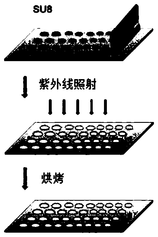
[0045] This embodiment relates to a method for preparing a silicon wafer template for the preparation of a microlens array structure, which is combined with figure 1 As shown in, the preparation method of the silicon wafer template specifically includes the following steps:

[0046] Step a: modifying the silicon wafer to make the surface of the silicon wafer non-wetting;

[0047] Step b: preparing circular patterns arranged in an array on the surface of the non-wetting silicon wafer to form a patterned surface;

[0048] Step c: coating SU8 photoresist on the patterned surface to form an array of SU8 photoresist droplets;

[0049] Step d: Expose to ultraviolet light and heat at 95° C. to obtain a silicon wafer template with a cured SU8 convex lens array.

[0050]Among them, in the above preparation steps, step a preferably uses 1H, 1H, 2H, 2H-perfluorooctyltriethoxysilane (POTS) to modify the silicon wafer, and step b preferably uses photolithography technology in a non-wetti...

Embodiment 2

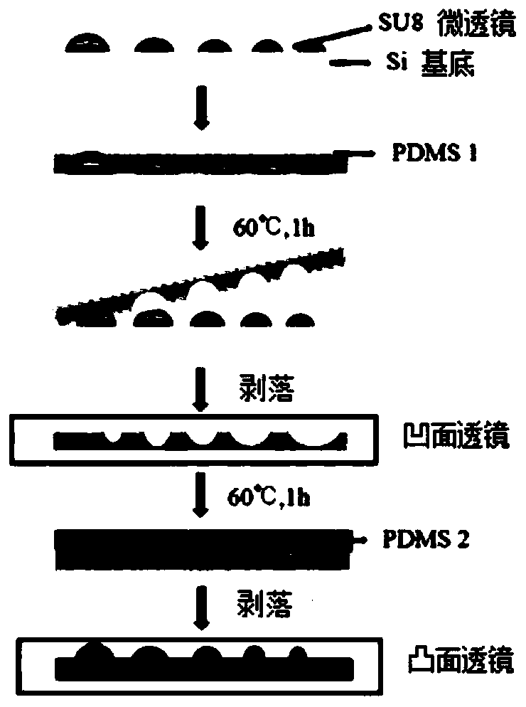
[0062] This embodiment relates to a preparation method of a microlens array structure, which method includes firstly adopting the preparation method in Embodiment 1 to prepare a silicon wafer template with a cured SU8 convex lens array, and as figure 2 As shown, the preparation method of the microlens array structure in this embodiment further includes:

[0063] Step e: Mix the PDMS prepolymer and the curing agent in a mass ratio of 10:1 and stir evenly, remove the air bubbles and pour it on the silicon wafer template with the SU8 convex lens array, and place it at room temperature to fully spread the PDMS;

[0064] Step f: heating and curing at 60° C., uncovering the poured PDMS to obtain a flexible PDMS microlens array, and the microlens array is a concave lens array.

[0065] Among them, the prepolymer and curing agent of the above-mentioned PDMS are also the main agent and curing agent mentioned in other appellations, and after the prepolymer and curing agent are mixed ev...

Embodiment 3

[0097] This embodiment relates to a protective film containing a microlens array, which can be used for LED lighting equipment, and electronic products such as mobile phones, tablet computers, smart watches, displays, etc. The display screen is protected to reduce or avoid external damage.

[0098] The protective film of this embodiment has a film-like substrate layer, and in addition to the substrate layer, like the existing commonly used screen protective film such as mobile phones, the protective film of this embodiment also includes the substrate layer of course. Other functional layers such as release film are attached to the surfaces on both sides to achieve different protective properties of the protective film. In addition, for the display screen protection screen of this embodiment, its main inventive point is that a microlens array is prepared on the substrate layer, so that the light transmittance of the protective film can be increased, thereby improving the applic...


PUM

PropertyMeasurementUnit
Diameteraaaaaaaaaa
Diameteraaaaaaaaaa

Abstract

The invention provides a preparation method of a silicon wafer template for preparing a micro-lens array structure. The method comprises the steps of modifying a silicon wafer to enable the surface ofthe silicon wafer to have non-wettability, preparing circular patterns arranged in an array on the surface of the non-wet silicon wafer to form a patterned surface, coating the patterned surface withSU8 photoresist to form an SU8 photoresist droplet array, performing exposing with ultraviolet light, and performing heating at 95 DEG C to obtain a silicon wafer template with a cured SU8 convex lens array. The invention also provides a preparation method of a micro-lens array structure using the silicon wafer template, and a protective film containing the micro-lens array. The preparation method of the silicon wafer template is simple, the prepared silicon wafer template can be repeatedly used, and the preparation cost can be reduced.

Description

technical field [0001] The present invention relates to the field of microfluidic technology, in particular to a method for preparing a silicon wafer template used for the preparation of a microlens array structure, and at the same time, the present invention also relates to a method for preparing a microlens array structure, and a microlens array-containing template protective film. Background technique [0002] Microlens arrays (MLAs) are arrays composed of lenses with clear apertures and relief depths of micron scale, which can be divided into two types: refractive microlens arrays and diffractive microlens arrays. It has basic functions, and has the characteristics of small unit size and high integration, so that it can complete the functions that traditional optical components cannot complete, and can constitute many new optical systems. As a functional component, it is used in wavefront sensing, light concentration , light shaping and other systems can be widely used....

Claims


Application Information

Patent Timeline
IPC IPC(8): G02B3/00
CPCG02B3/0018
Inventor 巫金波丁叶凯温维佳薛厂张萌颖林银银
Owner SHANGHAI UNIV
Learn More