Supercharge Your Innovation With Domain-Expert AI Agents!

Epitaxial method of overweight red phosphorus-doped substrate

A technology of substrate and red phosphorus, applied in the direction of electrical components, semiconductor/solid-state device manufacturing, circuits, etc., can solve the problems of lower yield, unable to solve the problems of gas phase doping composition, difference between epitaxial wafer edge and central SRP, etc., and achieve improvement The effect of yield

Inactive Publication Date: 2020-07-14
SHANGHAI JINGMENG SILICON CORP
View PDF8 Cites 1 Cited by
  • Summary
  • Abstract
  • Description
  • Claims
  • Application Information

AI Technical Summary

Problems solved by technology

However, this isolation method can only solve the self-doping between the substrate and the epitaxial layer, and cannot solve the influence of the gas phase doping composition and concentration on the resistivity, especially for the epitaxial process of the super heavily doped red phosphorus substrate. , the doping composition has a great influence on the resistivity, and the doping composition in the gas phase will cause a significant difference in the SRP between the edge and the center of the epitaxial wafer, resulting in a decrease in yield

Method used


Image

  • Epitaxial method of overweight red phosphorus-doped substrate
  • Epitaxial method of overweight red phosphorus-doped substrate
  • Epitaxial method of overweight red phosphorus-doped substrate

Examples


Embodiment 1

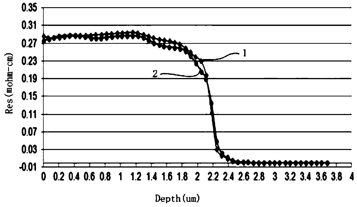
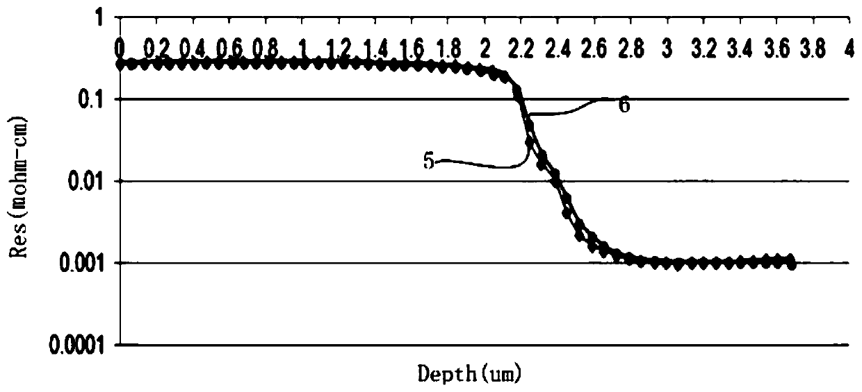
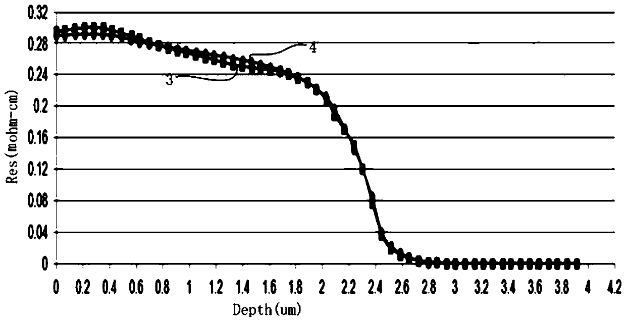
[0030] Step 1: Baking (BAKE) the substrate. The substrate is also referred to as the substrate. The substrate body and the main body of the epitaxial layer are composed of the same element, which is silicon. The substrate in this embodiment is a heavily doped phosphorus substrate, and the resistivity of the substrate is ≤1.0mohm-cm.

[0031] Step 2, growing an intrinsic silicon layer (CAP) with a thickness exceeding the required thickness on the super-heavily doped red phosphorus substrate to absorb impurities in the gas phase. The intrinsic silicon layer is formed by the reaction of trichlorosilane and hydrogen. That is, the single crystal silicon formed by the reaction is deposited on the upper surface of the substrate body to form the intrinsic silicon layer. In this embodiment, the thickness of the intrinsic silicon layer is not higher than 20% of the thickness of the substrate, preferably not higher than 10% of the thickness of the substrate. The required thickness of ...


PUM


Abstract

The invention relates to an epitaxial method of an overweight red phosphorus-doped substrate, and the method comprises the following steps: growing an intrinsic silicon layer with the thickness exceeding the required thickness on the overweight red phosphorus-doped substrate to absorb impurities in a gas phase, etching the intrinsic silicon layer to the required thickness, and carrying out epitaxyon the intrinsic silicon layer. The method is completely different from the isolation thought in the prior art; impurities in a gas phase are absorbed by generating an over-thick intrinsic silicon layer; compared with the prior art, the method has the advantages that the doping in the gas phase is effectively removed, the problem that the gas phase doping greatly influences the resistivity in theepitaxial process of the overweight red phosphorus-doped substrate is solved, the edge of the epitaxial wafer prepared by the epitaxial method is highly consistent with the SRP in the center, and theyield of products is improved.

Description

technical field [0001] The invention relates to a production method of an epitaxial wafer, in particular to an epitaxial method of a super-heavily doped red phosphorus substrate. Background technique [0002] In the production process of epitaxial wafers in the prior art, self-doping phenomena generally exist. Self-doping is due to thermal evaporation or the diffusion of the by-products of chemical reactions to the substrate. The silicon and impurities in the substrate enter the gas phase, changing the doping composition and concentration in the gas phase, resulting in the actual impurity in the epitaxial layer. A phenomenon in which a distribution deviates from an ideal situation. The self-doping phenomenon is serious in epitaxy of super-heavily doped red phosphorus substrates (substrate resistivity ≤ 1.0mohm-cm). resistance profile, the shape of the extended resistance curve) is significantly different. [0003] Chinese patent application document CN106505093A discloses...

Claims


Application Information

Patent Timeline
Patent Type & Authority Applications(China)
IPC IPC(8): H01L21/306H01L21/02
CPCH01L21/02381H01L21/0245H01L21/02532H01L21/02634H01L21/30604
Inventor 韩少锋顾广安陈建纲
Owner SHANGHAI JINGMENG SILICON CORP
Features
  • R&D
  • Intellectual Property
  • Life Sciences
  • Materials
  • Tech Scout
  • Unparalleled Data Quality
  • Higher Quality Content
  • 60% Fewer Hallucinations
Learn More