Antenna integrated packaging method and structure

An integrated packaging and antenna technology, applied in the direction of antenna, antenna support/mounting device, antenna components, etc., can solve problems affecting antenna performance and achieve the effect of increasing the application range

Active Publication Date: 2020-07-24
NAT CENT FOR ADVANCED PACKAGING
View PDF7 Cites 1 Cited by
  • Summary
  • Abstract
  • Description
  • Claims
  • Application Information

AI Technical Summary

Problems solved by technology

[0003] The purpose of the present invention is to provide a method and structure for antenna integrated packaging, to solve the problem of the large dielectric constant Dk and mater

Method used


Image

  • Antenna integrated packaging method and structure
  • Antenna integrated packaging method and structure
  • Antenna integrated packaging method and structure

Examples


Example Embodiment

[0073]

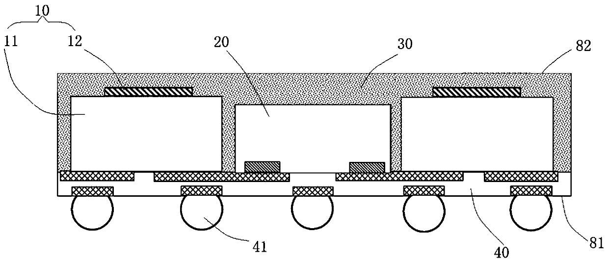
[0074] This embodiment provides an antenna integrated packaging structure, such as figure 2 As shown, the antenna integrated packaging structure includes a plurality of low-k dielectric and antenna patch integrated modules 10, a device die 20, a molding material 30, and a signal wiring layer 40, wherein: a plurality of the low-k dielectric and antenna patch integrated modules 10 The antenna patch integrated module 10 is distributed around the device die 20; the signal wiring layer 40 is located on the first plane 81 of the antenna integrated packaging structure, and the device die 20 is electrically connected to the signal wiring layer 40; The low-k dielectric and antenna patch integrated module 10 includes the low-k dielectric material 11 facing the first plane 81 of the antenna integrated packaging structure and the antenna patch 12 facing the second plane 82 of the antenna integrated packaging structure, The signal wiring layer 40 and the antenna patch 12 are separa...

Example Embodiment

[0083]

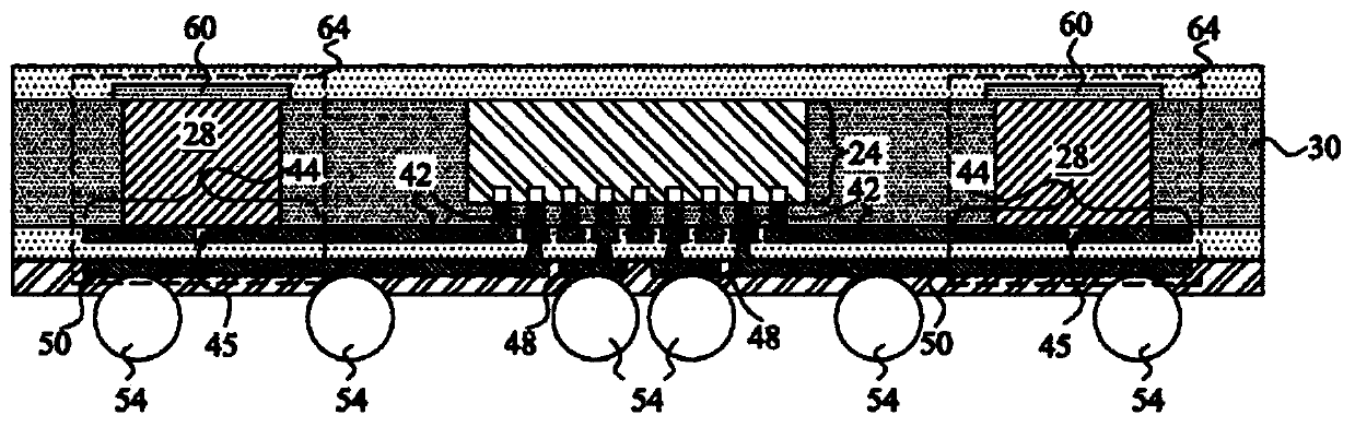
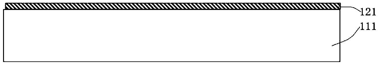
[0084] This embodiment provides an antenna integrated packaging method, such as Figure 3-14 As shown, Figure 3 to Figure 14 It is a cross-sectional view of an intermediate stage according to some exemplary embodiments. The antenna integrated packaging method includes: Figure 3~8 As shown, a low-k dielectric and antenna patch integrated module 10 is fabricated. The low-k dielectric and antenna patch integrated module 10 includes a low-k dielectric material 11 and an antenna patch 12; Picture 9 As shown, the device die 20 and the low-k dielectric and antenna patch integrated module 10 are placed above the first carrier 70; Picture 10 As shown, the device die 20 and the low-k dielectric and antenna patch integrated module 10 are molded in a molding material 30, the molding material 30, the device die 20, and the low-k dielectric The antenna patch integrated module 10 forms an antenna functional module 600; such as Picture 11 As shown, the antenna function module 600 ...


PUM


Abstract

The invention provides an antenna integrated packaging method and structure. The antenna integrated packaging method comprises: manufacturing a low-k dielectric and antenna patch integrated module comprising a low-k dielectric material and an antenna patch; placing a device pipe core and the low-k dielectric and antenna patch integrated module above a first carrier; molding the device pipe core and the low-k dielectric and antenna patch integrated module in a molding material, wherein the molding material, the device pipe core and the low-k dielectric and antenna patch integrated module form an antenna function module; taking down the antenna function module from the first carrier to expose the first plane of the antenna function module; forming a signal wiring layer on the first plane ofthe antenna function module, wherein the signal wiring layer is electrically connected with the device pipe core; thinning the second plane of the antenna function module, wherein the second plane ofthe antenna function module is spatially opposite to the first plane of the antenna function module; and forming a radio frequency signal propagation path from the low-k dielectric and antenna patch integrated module, the signal wiring layer and the device pipe core.

Description

technical field [0001] The invention relates to the technical field of semiconductors, in particular to an antenna integrated packaging method and structure. Background technique [0002] In the integrated fan-out package of RF millimeter-wave chips and antennas, the performance of the antenna is affected by the large dielectric constant Dk and material dissipation factor Df of the plastic packaging material, such as the document DOI10.1109 / ECTC.2018.00039 "InFO_AiPTechnology for High Performance and Compact 5G Millimeter Wave System Integration” discloses an INFO-based wafer-level fan-out antenna integration technology. The feeder needs to be coupled to the antenna patch through the plastic packaging material. The Dk and Df of the plastic packaging material are relatively large, and the gain and bandwidth of the antenna are limited. Contents of the invention [0003] The purpose of the present invention is to provide a method and structure for antenna integrated packaging...

Claims


Application Information

Patent Timeline
IPC IPC(8): H01L21/52H01L21/56H01L23/18H01L23/31H01L23/498H01L23/66H01Q1/22H01Q1/38
CPCH01L21/52H01L21/568H01L23/18H01L23/31H01L23/49838H01L23/66H01Q1/2283H01Q1/38H01L2223/6677H01L2224/18H01L2224/16225
Inventor 王全龙曹立强陈峰
Owner NAT CENT FOR ADVANCED PACKAGING
Why Eureka
Try Eureka