Optical chip and manufacturing method thereof

An optical chip and manufacturing method technology, applied in the field of optics and neural networks, can solve the problems of high integration, inability to implement, and cannot be carried, and achieve the effects of large integration, increased production capacity, and reduced cost

Inactive Publication Date: 2020-07-28
CHINA JILIANG UNIV
View PDF3 Cites 4 Cited by
  • Summary
  • Abstract
  • Description
  • Claims
  • Application Information

AI Technical Summary

Problems solved by technology

[0003] However, in this article, the wave plate is used to achieve optical modulation, because the size of the wave plate is usually relatively large, which leads to problems such as the inability to achieve a high degree of integration and portability in this way

Method used


Image

  • Optical chip and manufacturing method thereof
  • Optical chip and manufacturing method thereof
  • Optical chip and manufacturing method thereof

Examples


Embodiment Construction

[0030] Below in conjunction with the accompanying drawings, the technical scheme of the present invention will be described in detail.

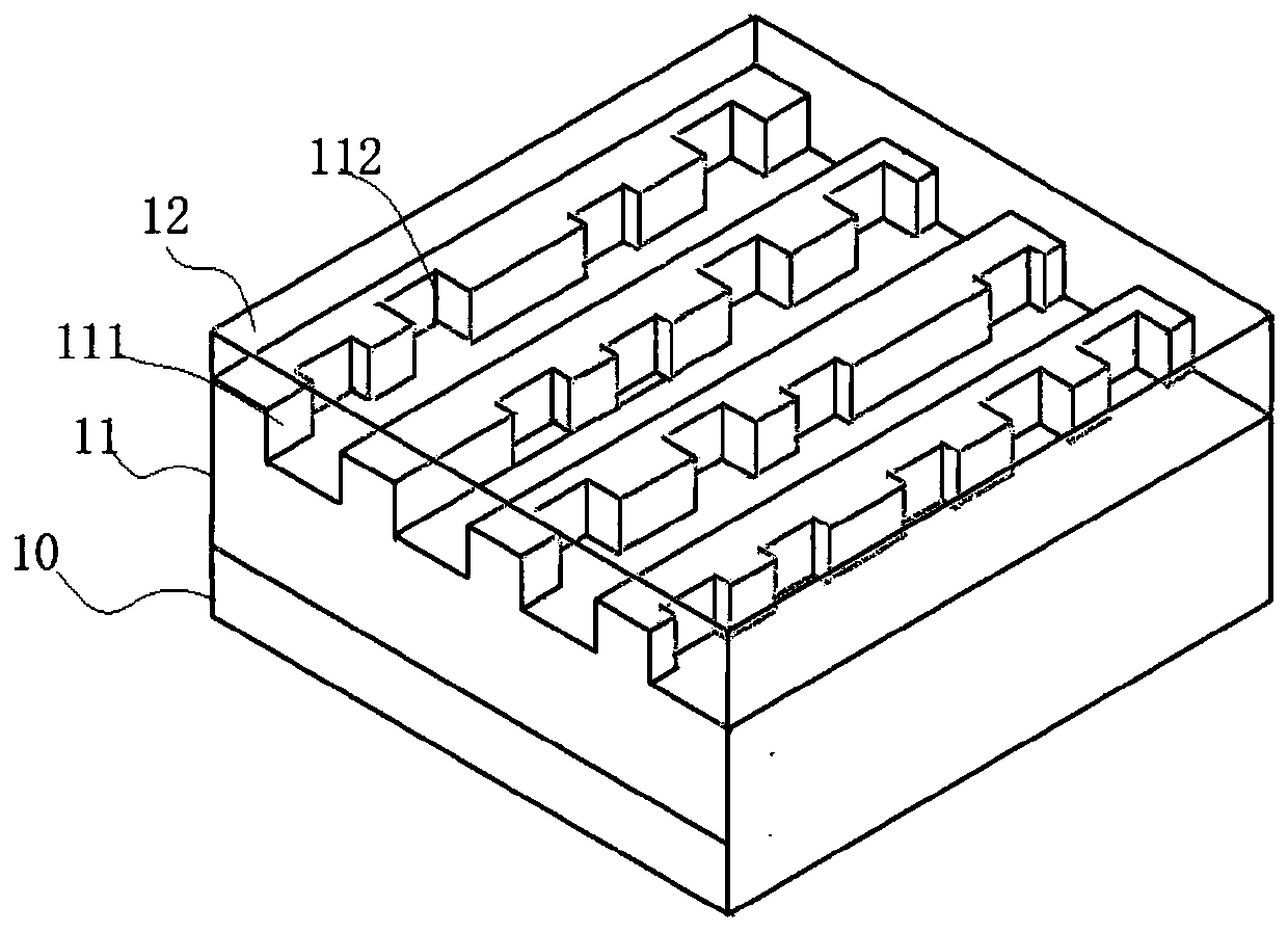
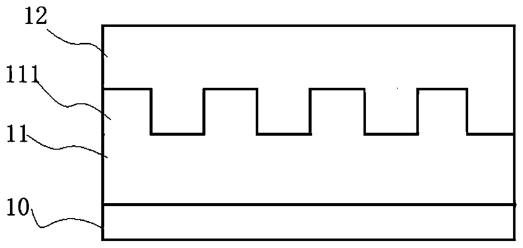
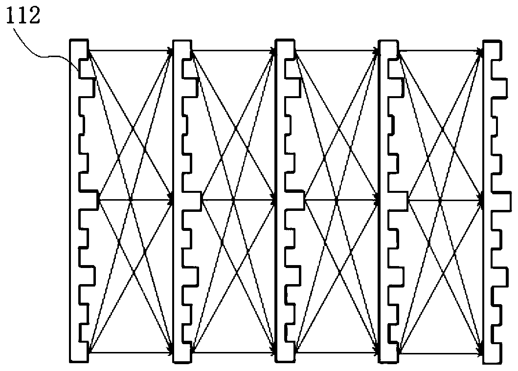
[0031] See figure 1 and figure 2 , figure 1 is the structural schematic diagram of the optical chip of the present invention, figure 2 It is a front view of the optical chip of the present invention. As shown in the figure, the optical chip includes a base layer 10 , a functional layer 11 and a cladding layer 12 . The functional layer is located on the base layer 10 , and the cladding layer covers the functional layer 11 .

[0032] The base layer 10 is a carrier material, which depends on the manufacturing process of the optical chip. For example, when the optical chip is manufactured by 3D printing technology, the carrier material can be a light-transmitting 3D printing material, such as ABS, PLA, ceramic powder, etc.; when the optical chip is made by a semiconductor lithography process, the carrier material can be a light-transmittin...


PUM


Abstract

The invention discloses an optical chip and a manufacturing method thereof. Machine learning is performed by designing an all-optical diffraction deep neural network architecture. According to the architecture, various functions can be realized on the basis of joint work of passive diffraction layers based on deep learning; an all-optical neural network architecture is made into an integrated chipby a grating based on a 3D printing technology, a specific task of training can be executed at a light speed, powerful functions can be realized by only using optical diffraction and passive opticalcomponents or layers, and the working efficiency is greatly improved. The invention also discloses an optical identification device.

Description

technical field [0001] The invention relates to the fields of optics and neural networks, in particular to an optical chip and a manufacturing method. Background technique [0002] In recent years, machine learning is bringing about a new technological change, which has greatly promoted our production and life. With the advent of the era of artificial intelligence, the hardware level and algorithm level in machine learning are also facing facing severe challenges. The previous electronic neural network can no longer meet the requirements of the development of the current era, and a new method is urgently needed to solve this problem. In the article "All-optical machine learning using diffractive deep neural networks" published by Xin Lin et al., a method for implementing machine learning with an optical scheme is mentioned. In this article, a set of waveplate diffraction layers are used to detect incident light. Modulation is performed, and then the display result is outpu...

Claims


Application Information

Patent Timeline
Patent Type & Authority Applications(China)
IPC IPC(8): G02B5/18G06N3/067
CPCG02B5/1819G02B5/1842G02B5/1847G02B2005/1804G06N3/067
Inventor 郝然梁星磊张飞金尚忠冯爱明陈义何建军
Owner CHINA JILIANG UNIV
Why Eureka
Try Eureka