Lossless single crystal wafer with edges convenient to identify, and marking method thereof, and special grinding wheel

A marking method and single-wafer technology, applied in the direction of bonded grinding wheel, laser welding equipment, electrical components, etc., can solve the problems of low processing efficiency, reduce processing damage rate, avoid axial processing, and increase the effect of effective use area

Pending Publication Date: 2020-07-28
哈尔滨科友半导体产业装备与技术研究院有限公司
View PDF21 Cites 0 Cited by
  • Summary
  • Abstract
  • Description
  • Claims
  • Application Information

AI Technical Summary

Problems solved by technology

[0003] In order to overcome the defect of low processing efficiency of the existing crystal plane marking method, the present invention provides a non-destructive single wafer whose edge is easy to identify and its marking method and special grinding wheel. The marking method reduces the damage to the crystal plane and improves the substrate Effectively utilized area of ​​crystal face and seed crystal face

Method used


Image

  • Lossless single crystal wafer with edges convenient to identify, and marking method thereof, and special grinding wheel
  • Lossless single crystal wafer with edges convenient to identify, and marking method thereof, and special grinding wheel
  • Lossless single crystal wafer with edges convenient to identify, and marking method thereof, and special grinding wheel

Examples


Embodiment 1

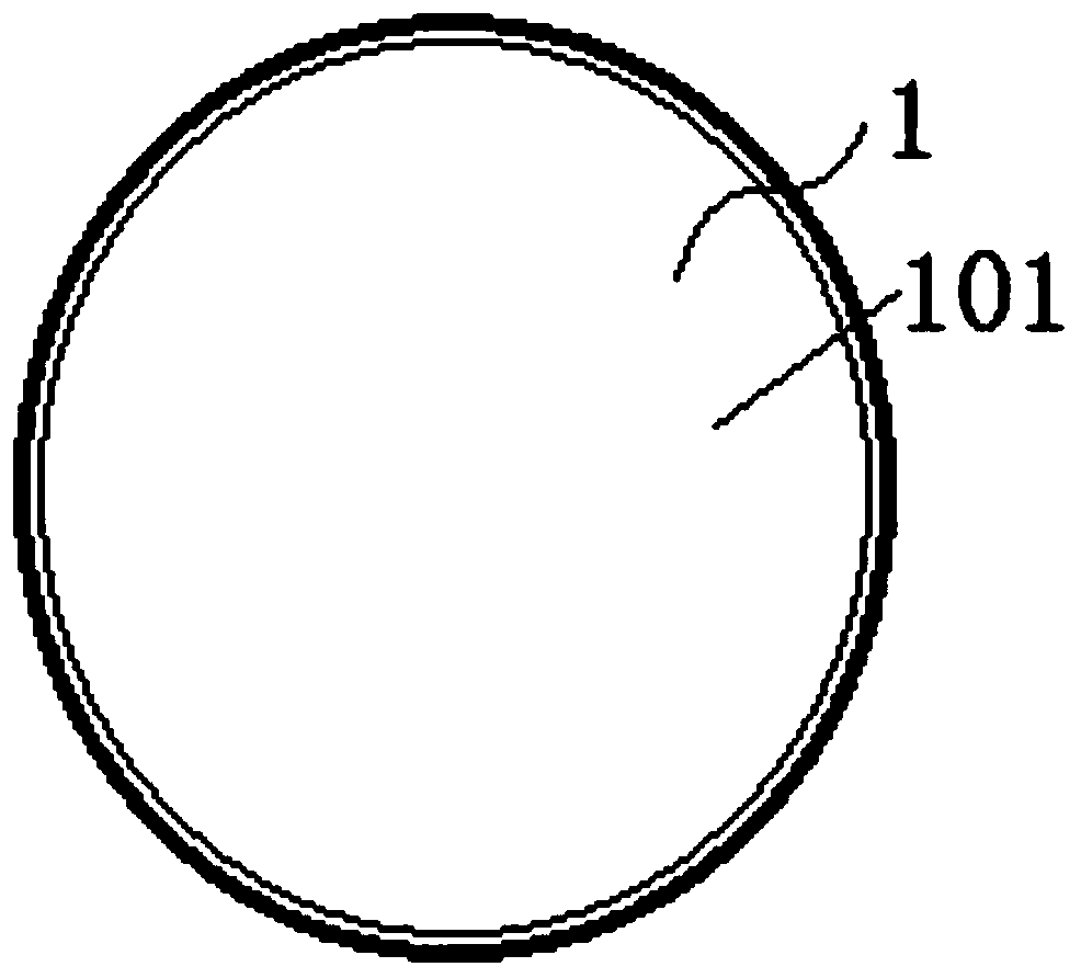
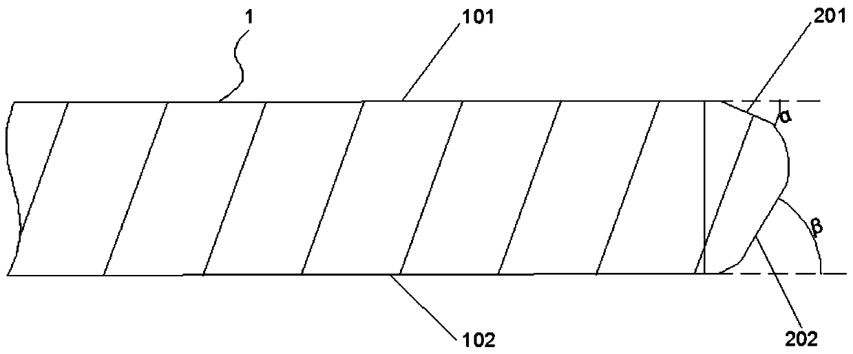
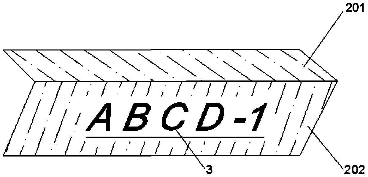
[0025] Such as Figure 1 to Figure 3 As shown, the present invention is a non-destructive single wafer whose edge is easy to identify, including a circular wafer body 1, which includes an upper surface 101 and a lower surface 102, and is processed at the edge of the wafer body 1 for identification. Chamfering 2, the chamfering 2 includes an upper bevel 201 and a lower bevel 202, the upper bevel 201 and the lower bevel 202 are asymmetrically arranged to avoid axial processing of the thinner wafer body 1 and reduce the processing damage rate. The upper bevel The intersection of 201 and upper surface 101 and the intersection of lower slope 202 and lower surface 102 are located on the same axis, so that the diameters of upper slope 201 and upper surface 101 are the same, which can increase the effective area of ​​wafer body 1 . Adjacent positions of the upper bevel 201 and the lower bevel 202 are connected by an outwardly protruding arc-shaped fillet, and this edge treatment metho...

Embodiment 2

[0028] On the basis of Embodiment 1, this embodiment is introduced by taking the wafer body 1 as an example of a silicon single crystal material.

[0029] The wafer body 1 can be used as a substrate wafer, the upper surface 101 is a front surface, and the lower surface 102 is a back surface. When the wafer body 1 is used as a substrate wafer, it is necessary to engrave an identifier 3 on the lower surface 102 with a laser, and the identifier 3 includes the direction of the crystal plane, the crystal orientation here, such as .

Embodiment 3

[0031] On the basis of Embodiment 1, this embodiment is introduced by taking the wafer body 1 as an example of silicon carbide single crystal material.

[0032] The wafer body 1 can be used as a wafer for a substrate or a wafer for a seed crystal, the upper surface 101 is a carbon plane (i.e. C plane, 000-1 plane), and the lower surface 102 is a silicon plane (i.e. Si plane, 0001 side). When the wafer body 1 is used as a substrate wafer, it is necessary to engrave an identifier 3 with a laser on the lower surface 102, and the identifier 3 includes a crystal plane direction, and the crystal orientation at this place, such as ; when the wafer body 1 When used as a wafer for a seed crystal, it is necessary to engrave an identifier 3 on the lower surface 102 with a laser, and the identifier 3 includes a crystal plane direction.


PUM

PropertyMeasurementUnit
thicknessaaaaaaaaaa

Abstract

The invention discloses a lossless single crystal wafer with an edge convenient to identify, and a marking method thereof, and a special grinding wheel, belongs to the technical field of semiconductorprocessing, and is provided for overcoming the defect that an existing single-wafer marking method is low in machining efficiency. The wafer comprises a wafer body, wherein the wafer body comprises an upper surface and a lower surface, chamfers used for identification are processed on an edge of the wafer body, the chamfer comprises an upper inclined surface and a lower inclined surface, the upper inclined surface is connected with the lower inclined surface through an arc-shaped fillet, an included angle formed between an extension line of the upper surface and an upper inclined plane is a first acute angle alpha, an included angle formed between an extension line of the lower surface and a lower inclined plane is a second acute angle beta, the first acute angle alpha is smaller than thesecond acute angle beta, the upper inclined plane and the lower inclined plane are asymmetrically arranged, the upper inclined plane and the upper surface have the same diameter, and identifiers areengraved on the lower inclined plane. The marking method comprises steps of cutting treatment, chamfering and edge polishing section treatment and marking treatment. The asymmetric chamfer is processed at an edge of the wafer body, an identifier is marked, so a processing damage rate is reduced, and an effective utilization area is increased.

Description

Technical field: [0001] The invention belongs to the technical field of semiconductor processing, and in particular relates to a non-destructive single wafer whose edge is easy to identify, a marking method thereof and a special grinding wheel. Background technique: [0002] Single crystal materials have different crystal planes, which have different physical properties. Semiconductor materials such as silicon Si, silicon carbide SiC and other single crystals are first processed into substrates with a thickness of hundreds of microns through cutting, grinding, polishing and other processes, and then epitaxy and device preparation are carried out on specific crystal planes. In the preparation process of crystal materials, it is also necessary to mark and distinguish crystal planes, because different crystal planes have different processing requirements. At present, the method of marking crystal planes is mainly to process a set of reference sides, main reference sides and su...

Claims


Application Information

Patent Timeline
Patent Type & Authority Applications(China)
IPC IPC(8): H01L21/02H01L23/544B23K26/362B23K26/402B24D5/00
CPCH01L21/02021H01L21/0201H01L21/02008H01L23/544B24D5/00B23K26/362B23K26/402H01L2223/544
Inventor 不公告发明人
Owner 哈尔滨科友半导体产业装备与技术研究院有限公司
Why Eureka
Try Eureka