Preparation method of hundred-micron two-dimensional organic rubrene monocrystal nanosheet

A single crystal nanometer and rubrene technology, which is applied in nanotechnology, ion implantation plating, coating and other directions, can solve the problem that nanometer cells cannot meet the requirements of macroscopic optical integrated circuit processing, and achieves simple operation and preparation cost. low effect

Inactive Publication Date: 2020-07-31
SHAOXING UNIVERSITY
View PDF0 Cites 0 Cited by
  • Summary
  • Abstract
  • Description
  • Claims
  • Application Information

AI Technical Summary

Problems solved by technology

At present, the size of one-dimensional organic nanowires and two-dimensional organic nanosheets prepared by the solution method usually ranges from

Method used


Image

  • Preparation method of hundred-micron two-dimensional organic rubrene monocrystal nanosheet
  • Preparation method of hundred-micron two-dimensional organic rubrene monocrystal nanosheet
  • Preparation method of hundred-micron two-dimensional organic rubrene monocrystal nanosheet

Examples


Embodiment

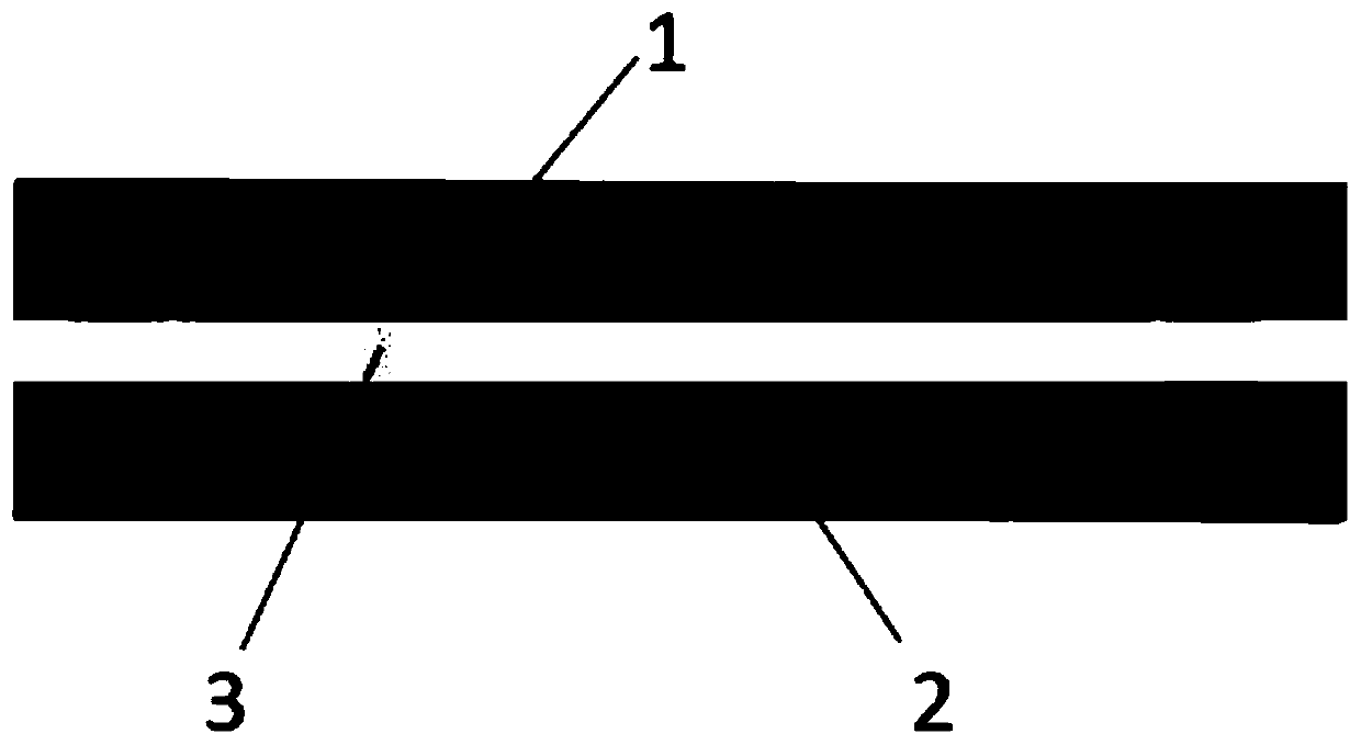
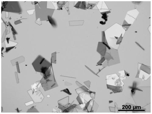
[0023] Embodiment: a kind of preparation method of two-dimensional organic rubrene single crystal nanosheet of hundred microns, such as Figure 1-Figure 7 Shown, described preparation method is:

[0024] Step 1. Preparation: prepare some ordinary silicon wafers, clean them with alcohol, and dry them with nitrogen for later use; grind rubrene into powder for later use;

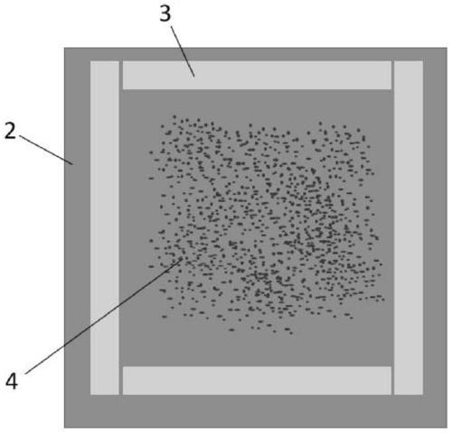
[0025] Step 2. Select two silicon wafers to form the evaporation unit. The size of the two silicon wafers is 1.5cm×1.5cm. The two silicon wafers are separated by four glass sheets of equal thickness. The allowable interval between the two silicon wafers is 30-60 microns, during evaporation, the above-mentioned evaporation unit is placed on a heating platform for heating, wherein the lower layer of silicon chip is the evaporation source carrier for carrying the evaporated rubrene powder, and the upper layer of silicon The sheet is the deposition substrate, which is used to carry the two-dimensional organic sing...


PUM


Abstract

The invention relates to a preparation method of a hundred-micron two-dimensional organic rubrene monocrystal nanosheet, and belongs to the technical field of hundred-micron two-dimensional organic monocrystal nanosheet preparation. According to the preparation method of the hundred-micron two-dimensional organic rubrene monocrystal nanosheet provided by the invention, the two-dimensional organicnanosheet with the size being larger than 100um can be prepared, no vacuum and complex device is needed in the whole evaporation process, and the preparation method of the hundred-micron two-dimensional organic rubrene monocrystal nanosheet has the characteristics of simplicity and convenience in operation, low preparation cost and the like. The rubrene nanosheet prepared by the invention has thetypical size being larger than 200 mum and the typical thickness ranging from 200 to 500 mum, and has an application value in the fields such as organic optical waveguide and organic laser.

Description

technical field [0001] The invention belongs to the technical field of preparation of two-dimensional organic single-crystal nanosheets of hundred micrometers, and in particular relates to a preparation method of two-dimensional organic rubrene single-crystal nanosheets of one hundred micrometers. Background technique [0002] Semiconductor low-dimensional micro-nanostructures (such as nanowires, nanosheets, etc.) have the ability to transmit and regulate light waves on a sub-wavelength scale, so they have broad application potential in the fields of organic light-emitting, micro-nano lasers, and optical waveguides. Nano-dimensional single crystals (such as one-dimensional nanowires and two-dimensional nanosheets) have light processing capabilities such as light capture, regulation, and transport. Therefore, these nanoscale single crystals constitute the basic building blocks of optical integrated circuits. In the industry, a "top-down" approach is usually used to prepare i...

Claims


Application Information

Patent Timeline
IPC IPC(8): C23C14/24C23C14/12B82Y40/00
CPCB82Y40/00C23C14/12C23C14/24
Inventor 窦卫东
Owner SHAOXING UNIVERSITY
Why Eureka
Try Eureka