
A method of manufacturing a patch power inductor

A technology of power inductors and manufacturing methods, which is applied in the field of inductors, can solve the problems of winding inductors and integrated inductors, poor inductance saturation characteristics, and low efficiency, and achieve high saturation characteristics, high-density packaging, and high efficiency. Effect

Active Publication Date: 2022-03-01
SHENZHEN MICROGATE TECH
View PDF2 Cites 0 Cited by
  • Summary
  • Abstract
  • Description
  • Claims
  • Application Information

AI Technical Summary

Problems solved by technology

However, due to the limitations of the manufacturing process, it is extremely difficult for wire-wound inductors and integral molded inductors to develop into smaller sizes.
Multilayer chip inductors are inductors made of multilayer printing technology. The internal conductive coil is silver conductor, which also needs to go through a high temperature sintering process. Therefore, the choice of magnetic powder materials is also limited, including ferrite powder and Some alloy powders with good high temperature resistance also have the problems of poor inductance saturation characteristics and low efficiency

Method used


Image

  • A method of manufacturing a patch power inductor
  • A method of manufacturing a patch power inductor
  • A method of manufacturing a patch power inductor

Examples


Embodiment Construction

[0028] A method for manufacturing a patch power inductor, the manufacturing process comprising the following steps:

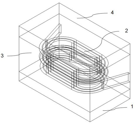
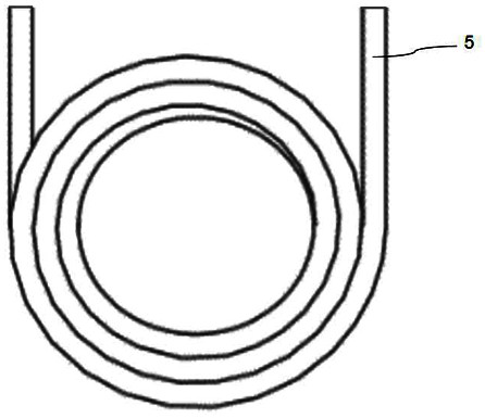
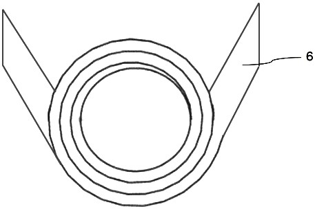
[0029] The first step: making the coil 2, winding the coil 2 by a winding machine, and then bending and stripping the pins 5 at both ends of the coil 2;

[0030] The second step: make the upper substrate 4 and the lower substrate 1, add organic matter to the powder, and make the upper substrate 4 and the lower substrate 1 through the ball milling process and casting method, the thickness of the upper substrate 4 and the lower substrate 1 are both 80-300μm;

[0031] The third step: make the magnetic printing layer 3, add organic matter to the powder, prepare the magnetic slurry through the milling process, print the magnetic slurry on the surface of the lower substrate 1 produced in the second step, and dry it at 60°C-80°C , repeat the printing step until the thickness of the printing layer reaches 350-450 μm;

[0032] The fourth step: placing the coil 2, plac...


PUM

PropertyMeasurementUnit
thicknessaaaaaaaaaa
thicknessaaaaaaaaaa
thicknessaaaaaaaaaa

Abstract

The invention relates to the field of inductors. At present, the field of inductor manufacturing has technical problems such as high sintering process temperature, few choices of magnetic powder materials, large size, and poor magnetic shielding performance. For this reason, the present invention provides a method for manufacturing chip power inductors, the manufacturing process of which includes the following steps: making a coil, making an upper substrate and a lower substrate, making a magnetic printing layer, placing the coil, placing the upper substrate, curing and cutting, the upper end electrodes and plating. Combining the winding process of integrally formed inductors and the multi-layer printing technology of laminated chip inductors, the production of chip inductors does not need to go through a high-temperature sintering process. Inductors have the advantages of small size, good magnetic shielding, high saturation characteristics, high efficiency, high-density packaging, and high production efficiency.

Description

technical field [0001] The invention relates to the field of inductors, in particular to a method for manufacturing chip power inductors combined with a winding process and a multi-layer printing technology. Background technique [0002] With the development of electronic components in the direction of miniaturization, low installation thickness, low electromagnetic interference and high efficiency, inductors must also cater to this trend. Therefore, it is an inevitable trend in the market to manufacture inductors with miniaturization, low electromagnetic interference, high inductance, high saturation characteristics and high efficiency. As one of the important categories of electronic components, SMD power inductors have the characteristics of high Q value, low impedance, and can provide tape packaging, etc., and are widely used in switching power supplies. The performance of the inductor will directly affect the performance of the switching power supply. For example, mini...

Claims


Application Information

Patent Timeline
Patent Type & Authority Patents(China)
IPC IPC(8): H01F41/04
CPCH01F41/041
Inventor 熊春美梁启新马龙侯志华周志斌
Owner SHENZHEN MICROGATE TECH
Learn More