A Virtual Multi-Channel SDRAM Access Method Supporting Flexible Block Access
An access method and multi-channel technology, applied in the field of virtual multi-channel SDRAM access, can solve problems such as large differences in performance characteristics, data loss, and large logic resource consumption, so as to improve versatility and portability, smooth data interaction, The effect of improving the utilization rate
- Summary
- Abstract
- Description
- Claims
- Application Information
AI Technical Summary
Problems solved by technology
Method used
Image
Examples
Embodiment 1
[0181] Block address calculation method
[0182] Since the main function of SDRAM is caching, the most common operation is to write sequentially and read sequentially. However, as the on-board tasks become more and more complex, different requirements are put forward for SDRAM access, such as requiring sequentially written data to follow A certain size is read in blocks. The main difficulty of the block read operation lies in the address calculation, because the sequential operation only needs one incremental counter to complete the addressing, and the block operation varies with the size and size of the storage space, and the address calculation method is bound to occur. Changes, complex address calculations will additionally consume limited computing resources on the star;
[0183] The present invention analyzes in detail the law of block address mapping under certain conditions, thereby proposing an extremely simple block address calculation method, the analysis process is...
Embodiment 2
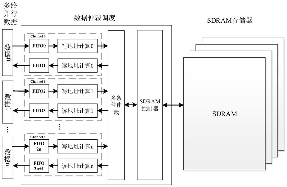
[0225] The following "SDRAM memory" means an external SDRAM storage device, "multi-channel parallel data" is user layer interface data; "data arbitration scheduling" is the main part of the access method of the present invention.
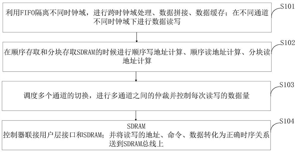
[0226] It mainly includes the following steps:
[0227]S1. FIFO isolation module: used for cross-clock domain processing and data splicing and caching, so as to adapt to simultaneous reading and writing in different channels and different clock domains, which increases the flexibility of the architecture and facilitates porting;
[0228] S2. Read and write address calculation: used for addressing calculations when accessing SDRAM sequentially and in blocks, including sequential write address calculations, sequential read address calculations, and block read address calculations;
[0229] Step S2 includes the following sub-steps:
[0230] S21. The data to be written is allocated to the address in the SDRAM, assuming that the array of the two-dimensi...
PUM
 Abstract
Description
Claims
Application Information


