Broadband terahertz wave absorber based on three-dart-shaped graphene
A graphene and wave absorber technology, applied in the field of terahertz metamaterial wave absorption, can solve problems such as low absorption efficiency, limited application, and narrow bandwidth
- Summary
- Abstract
- Description
- Claims
- Application Information
AI Technical Summary
Problems solved by technology
Method used
Image
Examples
Embodiment Construction
[0023] The present invention will be further described below in conjunction with specific examples.
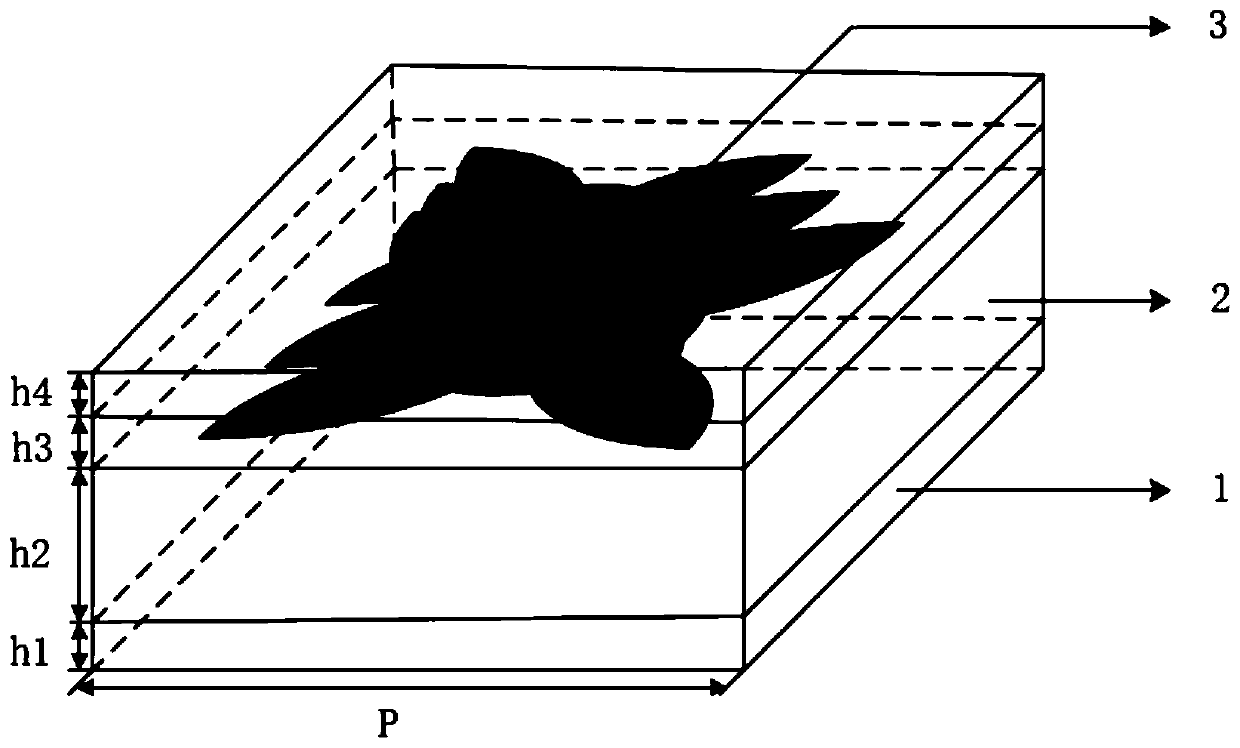
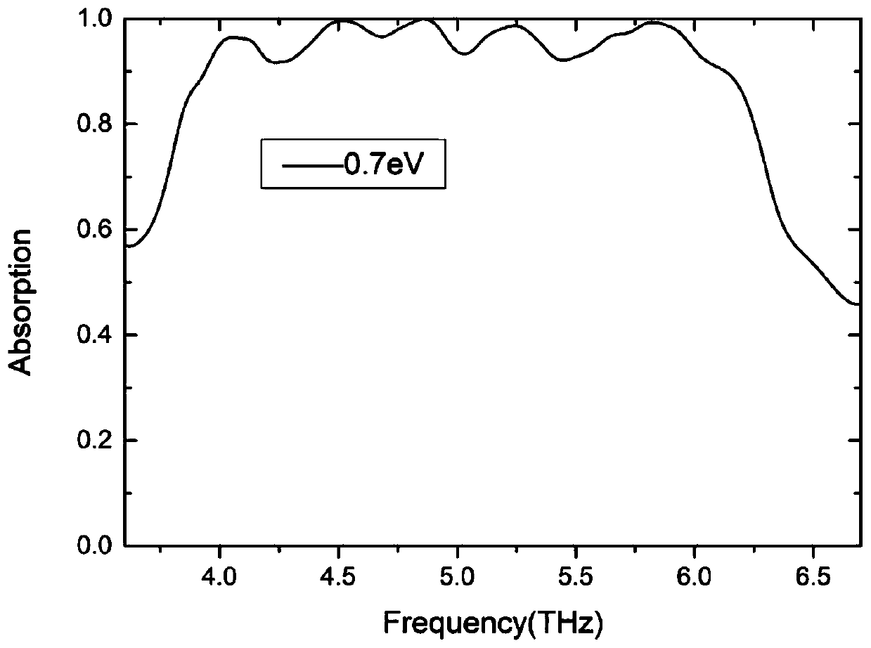
[0024] Such as figure 1 , 2 As shown, the present invention proposes a broadband terahertz absorber based on three "dart" shaped graphene. The device is composed of multiple absorbing units, and its main structure includes a bottom metal plate (1), a silicon dioxide dielectric layer (2), and three "dart"-shaped graphene layers (3), which are attached to each other. combine. The underlying metal film (1) is a gold film, and the three "dart"-shaped graphenes (3) are formed by adding dielectric silicon between each layer of "dart"-shaped graphene. The geometric centers of the absorbing units are on a straight line.
[0025] As an example, the structural dimensions of each absorbing unit are as follows: the lattice period is P=20000nm, the gold film thickness is h1=600nm, and the silicon dioxide thickness is h2=3000nm. , the three "dart" shaped graphenes are counted from bott...
PUM
| Property | Measurement | Unit |
|---|---|---|
| thickness | aaaaa | aaaaa |
| thickness | aaaaa | aaaaa |
| thickness | aaaaa | aaaaa |
Abstract
Description
Claims
Application Information


