Semiconductor packaging device

A technology for packaging devices and semiconductors, which is applied in the fields of semiconductor devices, semiconductor/solid-state device components, and electric solid-state devices, etc., can solve the problems of high cost, low stability of packaging devices, and high brittleness of silicon interposers, so as to improve performance and reduce Packaging cost, the effect of improving signal transmission rate

Pending Publication Date: 2020-08-18
NANTONG FUJITSU MICROELECTRONICS
View PDF4 Cites 3 Cited by
  • Summary
  • Abstract
  • Description
  • Claims
  • Application Information

AI Technical Summary

Problems solved by technology

[0002] In the semiconductor packaging device packaged by the existing chip packaging technology, the chip is usually connected to the substrate through a silicon interposer. The electrical performance and thermal conductivity of the semiconductor packaging device are excellent, but the cost is high, and the silicon interposer is relatively brittle. high, resulting in lower stability of the packaged device

Method used


Image

  • Semiconductor packaging device
  • Semiconductor packaging device
  • Semiconductor packaging device

Examples


Embodiment Construction

[0023] The following will clearly and completely describe the technical solutions in the embodiments of the present application with reference to the drawings in the embodiments of the present application. Obviously, the described embodiments are only some of the embodiments of the present application, not all of them. Based on the embodiments in this application, all other embodiments obtained by persons of ordinary skill in the art without making creative efforts belong to the scope of protection of this application.

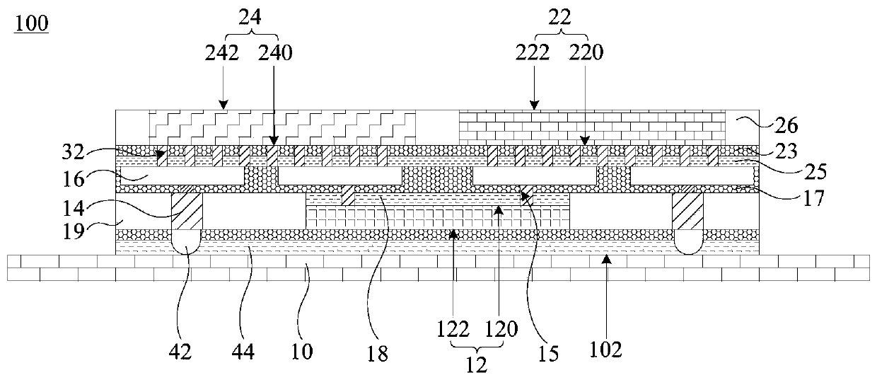
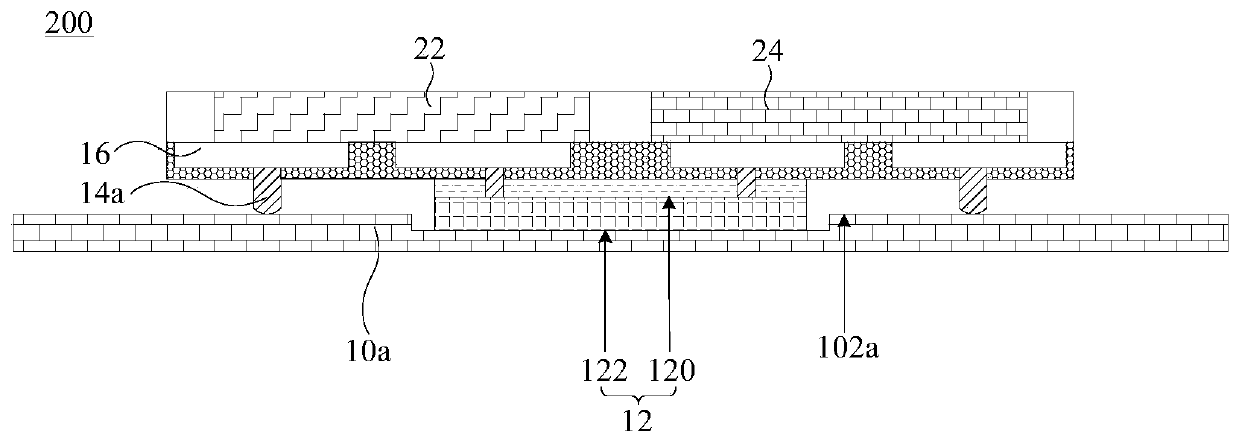
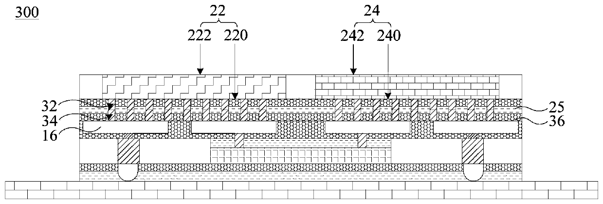
[0024] see figure 1 , figure 1 It is a schematic structural diagram of an embodiment of a semiconductor package device of the present application. The semiconductor package device 100 includes: a package substrate 10, a connecting chip 12, a plurality of first conductive pillars 14, at least one first rewiring layer 16, and a first chip 22. and the second chip 24 . Wherein, the connecting chip 12 includes a functional surface 120 and a non-functional surface...


PUM


Abstract

The invention discloses a semiconductor packaging device. The semiconductor packaging device comprises a packaging substrate, a connecting chip, a plurality of first conductive columns, at least one first rewiring layer, a first chip and a second chip. The connecting chip is located at one side of the packaging substrate, and the non-functional surface of the connecting chip faces the packaging substrate. The first conductive column is located at the periphery of the connecting chip, and one end of the first conductive column is electrically connected with the packaging substrate. The first rewiring layer is located at one side of the functional surface of the connecting chip, and different areas of the first rewiring layer are electrically connected with the connecting chip and the otherends of the first conductive columns respectively. The first chip and the second chip are arranged on the first rewiring layer in the same layer, the signal transmission areas on the functional surfaces of the first chip and the second chip are arranged close to each other, and the signal transmission areas and the non-signal transmission areas on the functional surfaces of the first chip and thesecond chip are the same in height and are electrically connected with the first rewiring layer. By the above mode, the packaging cost can be reduced, and the performance of the semiconductor packaging device can be improved.

Description

technical field [0001] The present application relates to the technical field of semiconductors, in particular to a semiconductor packaging device. Background technique [0002] In the semiconductor packaging device packaged by the existing chip packaging technology, the chip is usually connected to the substrate through a silicon interposer. The electrical performance and thermal conductivity of the semiconductor packaging device are excellent, but the cost is high, and the silicon interposer is relatively brittle. High, resulting in lower stability of the packaged device. Therefore, it is necessary to combine the advantages of existing packaging technologies to develop a new packaging technology to form a new semiconductor packaging device, which can reduce costs and form a semiconductor packaging device with excellent performance. Contents of the invention [0003] The technical problem mainly solved by this application is to provide a semiconductor packaging device, w...

Claims


Application Information

Patent Timeline
Patent Type & Authority Applications(China)
IPC IPC(8): H01L23/498H01L23/535H01L23/48H01L23/52H01L25/065
CPCH01L23/48H01L23/49811H01L23/49816H01L23/52H01L23/535H01L25/0655H01L2224/18
Inventor 石磊
Owner NANTONG FUJITSU MICROELECTRONICS
Why Eureka
Try Eureka