Longitudinal high voltage power semiconductor device structure with low relative dielectric constant buried layer

A relative permittivity, power semiconductor technology, applied in semiconductor devices, electrical components, circuits, etc., can solve the problem that the position of device breakdown still exists, the maximum electric field has not been significantly improved, etc., to improve on-resistance, increase Device performance, the effect of reducing power loss

Inactive Publication Date: 2020-08-18
陕西半导体先导技术中心有限公司
View PDF3 Cites 2 Cited by
  • Summary
  • Abstract
  • Description
  • Claims
  • Application Information

AI Technical Summary

Problems solved by technology

However, it does not significantly improve the maximum electric field in the device where the CC' channel is c

Method used


Image

  • Longitudinal high voltage power semiconductor device structure with low relative dielectric constant buried layer
  • Longitudinal high voltage power semiconductor device structure with low relative dielectric constant buried layer
  • Longitudinal high voltage power semiconductor device structure with low relative dielectric constant buried layer

Examples


Embodiment Construction

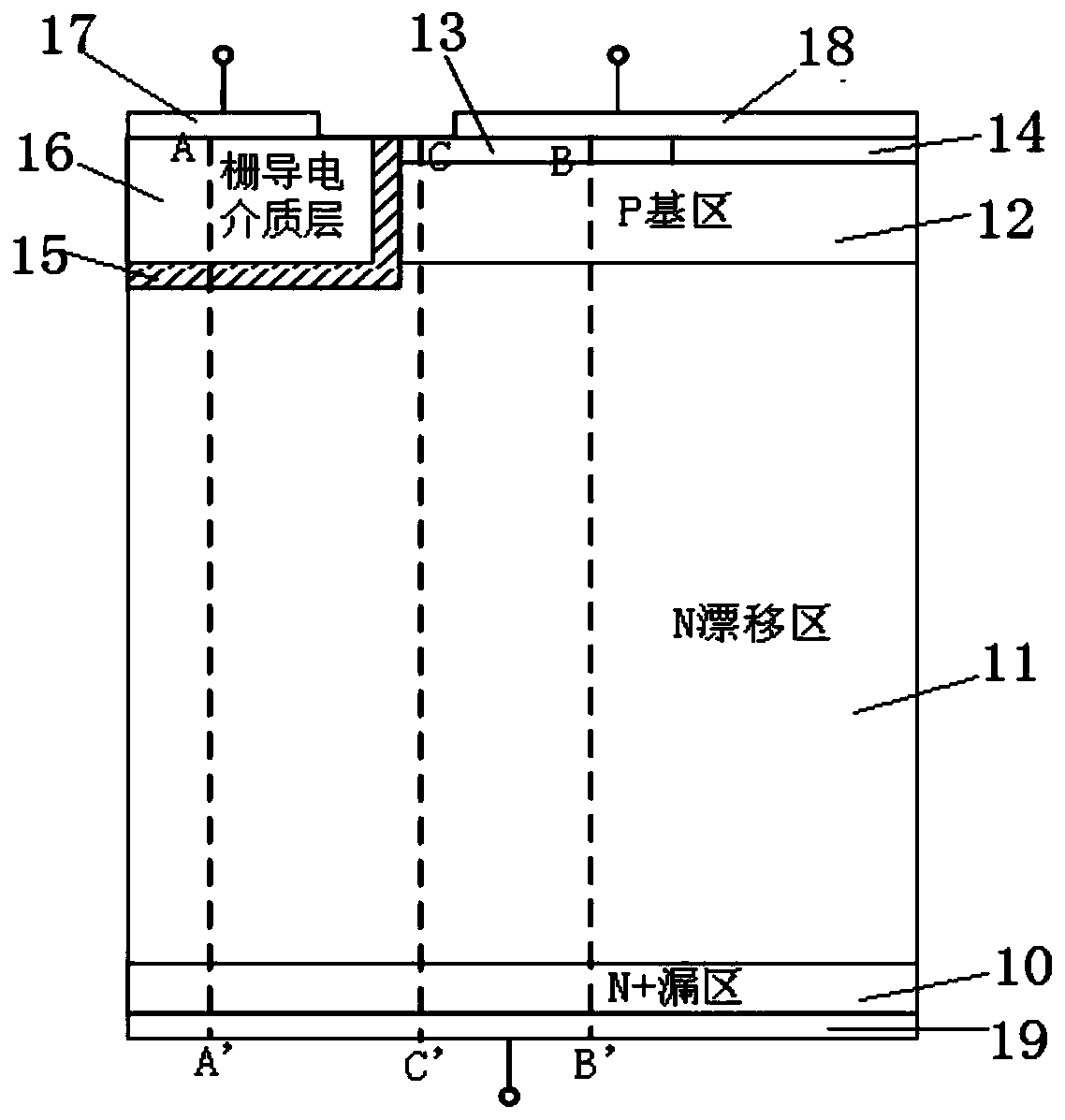
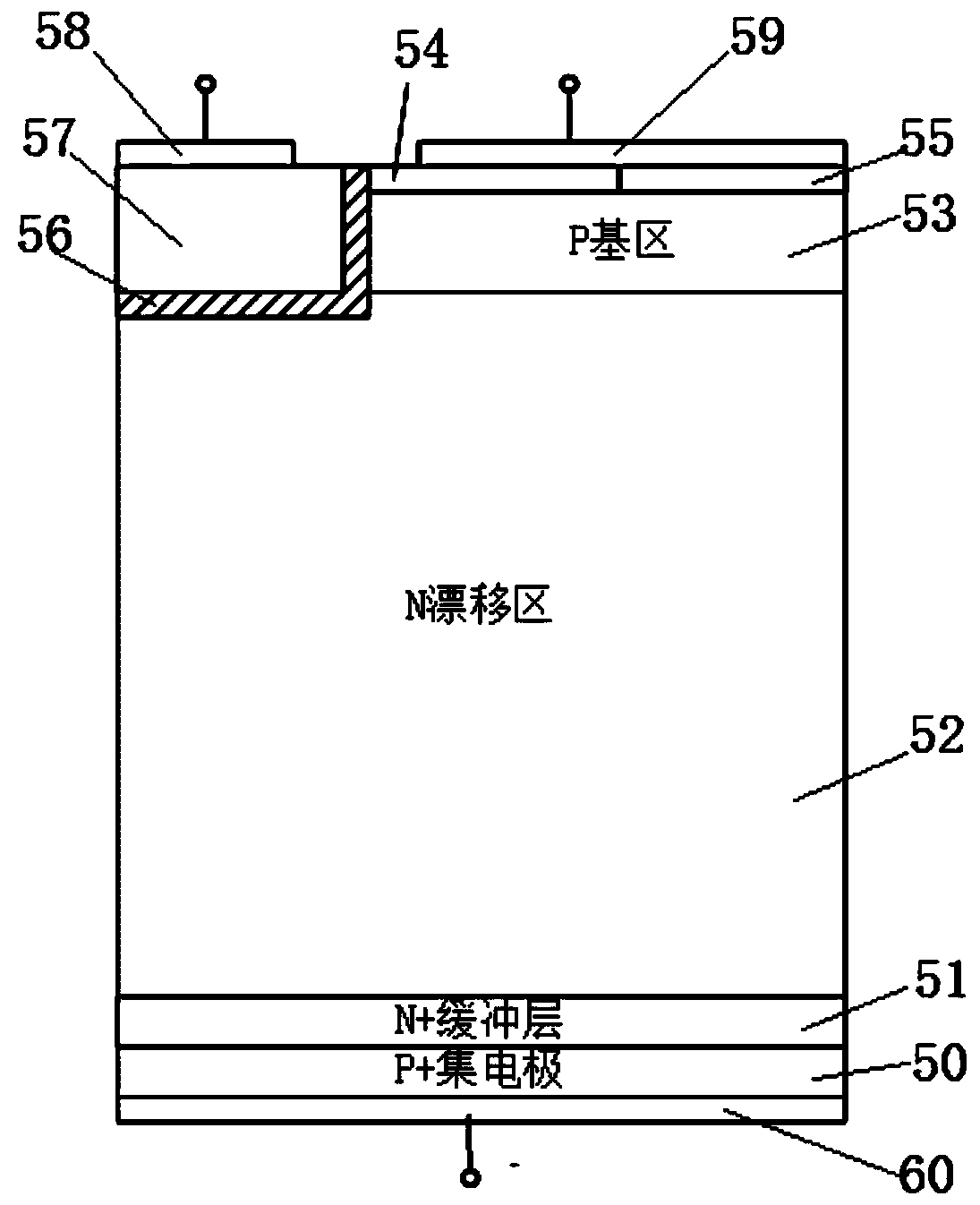
[0025] Aiming at the above technical solutions, preferred embodiments are given for specific description. Because the structure of the trench IGBT is essentially just adding a layer of P+ layer at the bottom of the trench MOS, and this part of the structure does not affect the withstand voltage performance of the device, only the trench MOS is used as the object for specific description. The principle of the IGBT is similar, not Let me repeat.

[0026] see Figure 6 , including N+ drain region 10, N drift region 11, P base region 12, N+ source region 13, P+ contact layer 14 on the silicon-based material from bottom to top, and at the same time, the N A gate oxide layer 15 is deposited in the device trench on the surface of the drift region, and then a gate conductive dielectric layer 16 is deposited. The material of the gate oxide layer is silicon dioxide, and the material of the gate conductive dielectric layer is polysilicon material. Metal is then deposited on the surface ...


PUM


Abstract

The invention discloses a longitudinal high-voltage power semiconductor device structure with a low relative dielectric constant buried layer. The semiconductor device structure comprises an N drift region, a P base region and an N+ source region, wherein a gate oxide layer is deposited in a trench at the periphery of the P base region and the N+ source region, and a gate conductive dielectric layer is deposited on the gate oxide layer. The semiconductor device structure is characterized in that an insulating layer is additionally arranged in the N+ drift region below the gate oxide layer; theinsulating layer is made of an insulating material of which the relative dielectric constant is less than that of the gate oxide layer; and the material of the device is Si, SiC or GaN. By additionally arranging the insulating layer with a certain thickness below the trench, the electric field distribution between the gate and the drain can be adjusted, so that the electric field distribution ofthe internal region of the device is changed, the withstand voltage of the device is also improved, and the electric field distribution in the device is not only limited by the doping concentration ofa material any more.

Description

technical field [0001] The invention relates to the technical field of power electronics, in particular to a semiconductor device structure for increasing withstand voltage and reducing on-resistance in vertical power semiconductor devices. Background technique [0002] Metal-Oxide-Semiconductor Field-Effect Transistor (MOSFET) is a field-effect transistor that can be widely used in analog circuits and digital circuits. It is a two-layer pn junction structure of npn or pnp. A gate electrode formed of an oxide layer and a conductive material is loaded on the middle semiconductor layer. The gate electrode can control the turn-on and turn-off of the MOS device, thereby realizing the circuit control. Because of its infinite gate input impedance (isolation of the gate oxide layer), MOS devices are more power-saving and easier to drive. They are not only widely used in digital signal processing occasions such as microprocessors and microcontrollers, but also more and more Ground...

Claims


Application Information

Patent Timeline
IPC IPC(8): H01L29/78H01L29/10H01L29/51
CPCH01L29/7827H01L29/512H01L29/1033
Inventor 张弦弓小武田力何晓宁陈晓炜田鸿昌
Owner 陕西半导体先导技术中心有限公司
Why Eureka
Try Eureka