A reconfigurable chip antenna based on tsv three-dimensional packaging and its reconfiguration method

A technology of chip antenna and three-dimensional packaging, which is applied in the direction of antenna grounding switch structure connection, antenna, slot antenna, etc., can solve the problems of high power consumption, single reconstruction variable, and high application complexity

Active Publication Date: 2021-10-26
NANJING UNIV OF AERONAUTICS & ASTRONAUTICS +1
View PDF9 Cites 0 Cited by
  • Summary
  • Abstract
  • Description
  • Claims
  • Application Information

AI Technical Summary

Problems solved by technology

However, there are disadvantages such as single refactoring variables, high power consumption, and high application complexity.

Method used


Image

  • A reconfigurable chip antenna based on tsv three-dimensional packaging and its reconfiguration method
  • A reconfigurable chip antenna based on tsv three-dimensional packaging and its reconfiguration method
  • A reconfigurable chip antenna based on tsv three-dimensional packaging and its reconfiguration method

Examples


Embodiment Construction

[0030] The technical solution of the present invention will be described in detail below in conjunction with the accompanying drawings and specific embodiments.

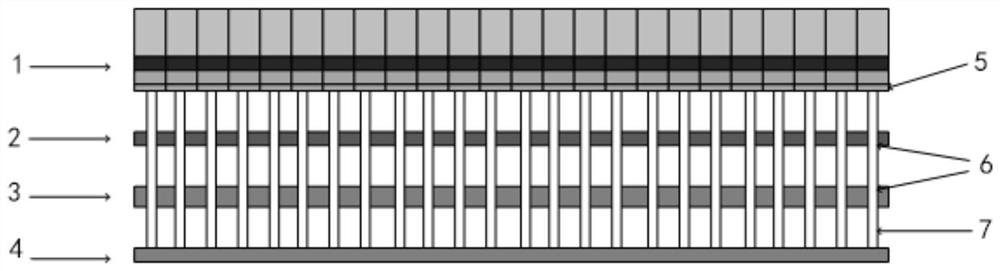
[0031] like figure 1 Shown is a schematic diagram of the structure of the antenna of the present invention, which is only to illustrate the positional relationship of each layer of the antenna of the present invention. In fact, each layer is tightly bonded together through the process. The antenna of the present invention mainly has a four-layer structure, which are respectively from top to bottom: a cross radiation layer 1, a metal cross slot layer 2, a reconfigurable feeding network layer 3, and a bias and control layer 4. The design of each level is described in detail below.

[0032] The cross radiation layer 1 of the present invention is composed of M×N silicon hole process diode arrays arranged in a criss-cross pattern, each row or column has a gap between the silicon hole process diode line arrays, and the or...


PUM


Abstract

The invention discloses a reconfigurable chip antenna based on TSV three-dimensional packaging and its reconfiguration method. The antenna includes a cross radiation layer, a metal cross slot layer, a reconfigurable feed network layer, and bias and control from top to bottom. Layer, the first bias line of the silicon hole process diode in the cross radiation layer is connected to the bias and control layer through the metal cross gap layer and the via hole on the reconfigurable feed network layer; the cross radiation layer is used for antenna radiation, embedded To the metal cross slot layer below; the metal cross slot layer is used to form two reconfigurable variables of frequency and polarization; the reconfigurable feed network layer is used to feed the bivariate reconfigurable antenna; the bias and control layer Used to arrange bias circuit and control circuit. Methods The frequency and polarization reconfiguration of the antenna is realized by controlling the conduction or cut-off of the S-PIN on the slits at different positions and the corresponding S-PIN of the reconfigurable feed network. The invention reduces chip power consumption and reduces invalid reflection of radio frequency signals.

Description

technical field [0001] The invention relates to antenna technology, in particular to a reconfigurable chip antenna based on TSV three-dimensional packaging and a reconfiguration method thereof. Background technique [0002] Through Silicon Via technology (Through Silicon Via, TSV) technology is a high-density packaging technology, which is gradually replacing the current relatively mature wire bonding technology, and is considered to be the fourth generation packaging technology. TSV technology realizes the vertical electrical interconnection of through-silicon holes by filling conductive substances such as copper, tungsten, and polysilicon. TSV technology can reduce interconnection length through vertical interconnection, reduce signal delay, reduce capacitance / inductance, realize low power consumption between chips, high-speed communication, increase broadband and realize miniaturization of device integration. [0003] Antenna is one of the core components of electronic s...

Claims


Application Information

Patent Timeline
Patent Type & Authority Patents(China)
IPC IPC(8): H01Q15/00H01Q1/36H01Q1/50H01Q5/30H01Q13/10H01Q15/24
CPCH01Q1/36H01Q1/50H01Q13/10H01Q15/002H01Q15/24H01Q5/30
Inventor 刘少斌胡智勇周永刚陈鑫安彤蒋海珊梁景原
Owner NANJING UNIV OF AERONAUTICS & ASTRONAUTICS
Why Eureka
Try Eureka