Supercharge Your Innovation With Domain-Expert AI Agents!

Row scanning circuit in CMOS image sensor

An image sensor and line scanning technology, which is applied in the field of line scanning circuits, can solve problems such as waste of power consumption, data errors, and large scale of strobe signal overlapping circuits, so as to reduce chip area and power consumption overhead, and reduce actual work The effect of time, high-speed accurate reading

Pending Publication Date: 2020-08-25
合肥海图微电子有限公司
View PDF7 Cites 1 Cited by
  • Summary
  • Abstract
  • Description
  • Claims
  • Application Information

AI Technical Summary

Problems solved by technology

[0012] The purpose of the present invention is to provide a line scan circuit in a CMOS image sensor, to solve the waste of power consumption and data errors in the line scan circuit in the prior art, and to use a controllable delay unit to process the gate signal. The overlapping circuit scale is large. , and high data bus driver requirements, difficult chip layout and other issues

Method used


Image

  • Row scanning circuit in CMOS image sensor
  • Row scanning circuit in CMOS image sensor
  • Row scanning circuit in CMOS image sensor

Examples


Embodiment Construction

[0044] The present invention will be further described below in conjunction with the accompanying drawings and embodiments.

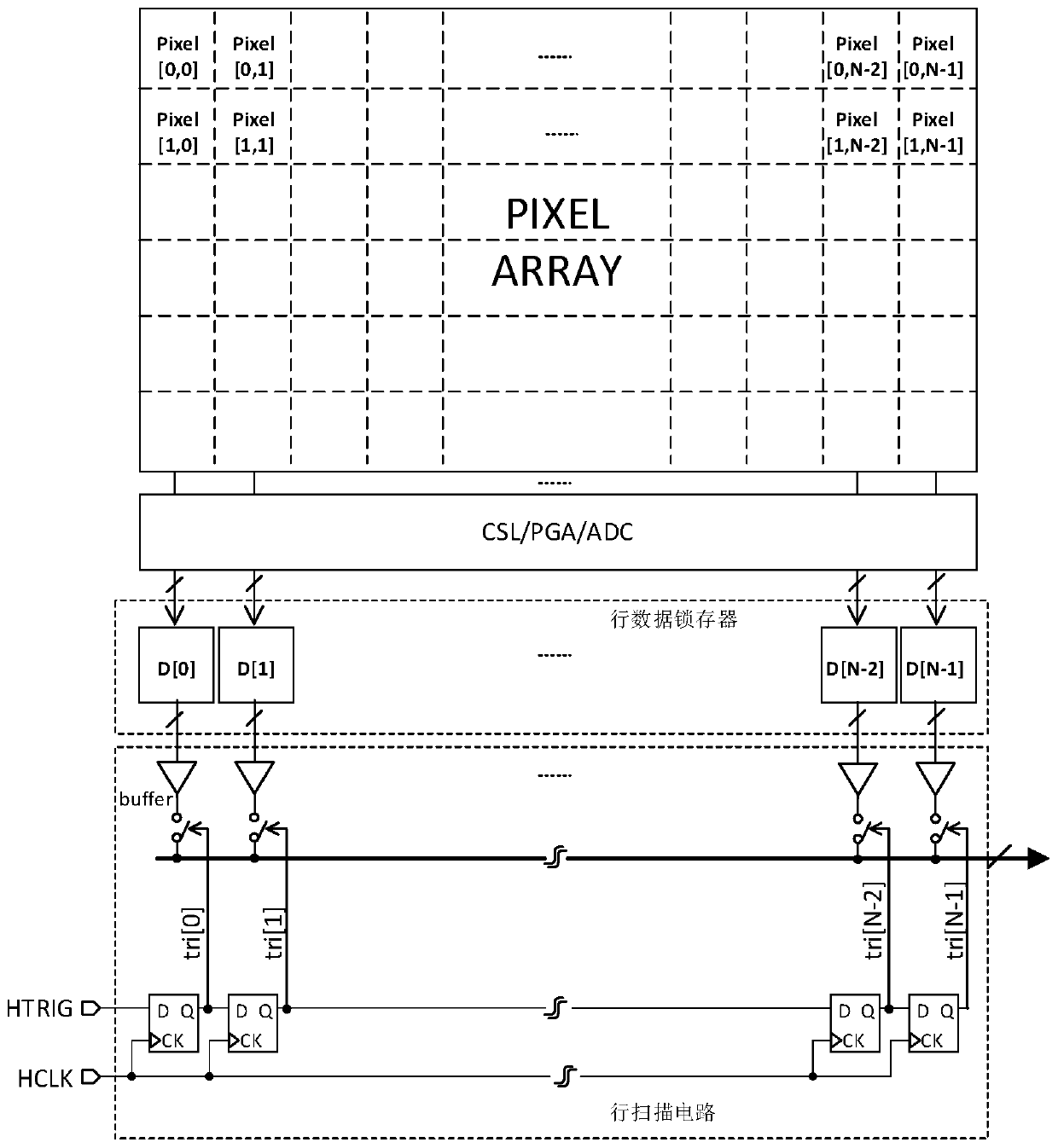
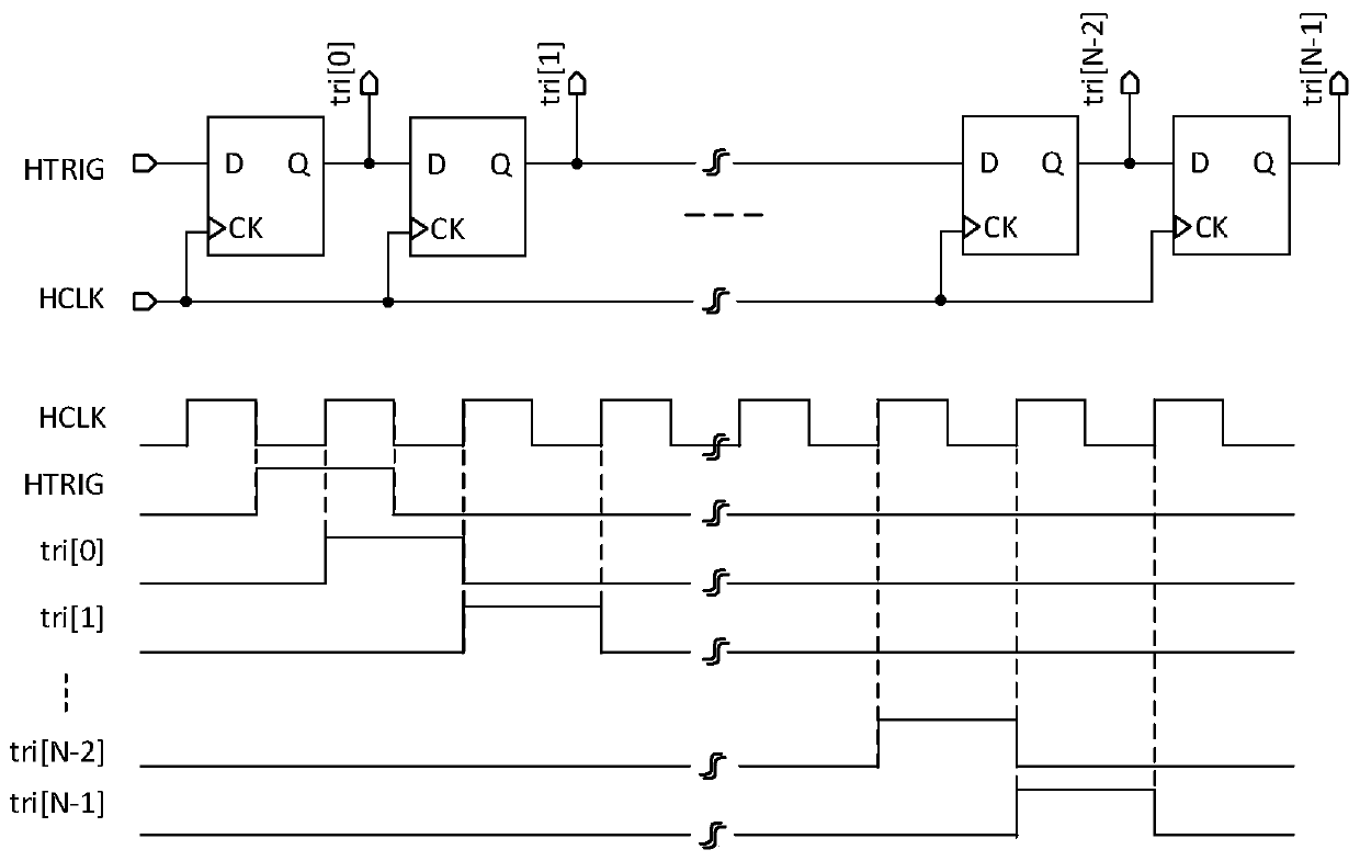
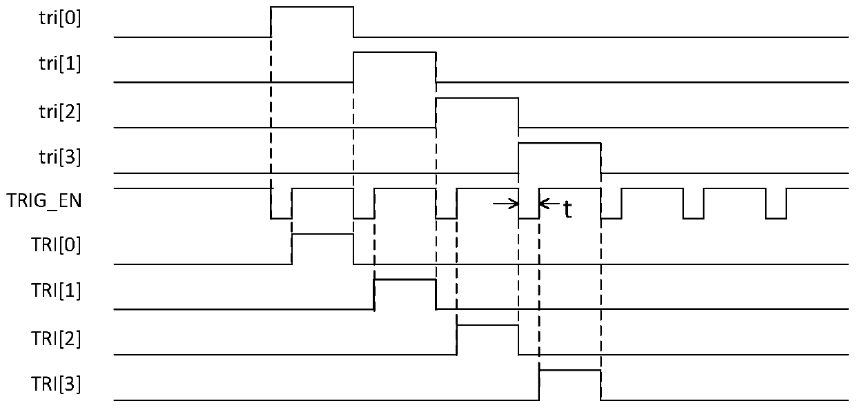
[0045] like Figure 6 ~ Figure 11 As shown, the row scanning circuit in a CMOS image sensor of the present invention includes a first module A composed of a shift register chain and a local clock control module, a second module B composed of a non-overlapping processing circuit array, and composed of The third module C constituted by the data bus driving circuit.

[0046] In the first module A, the shift register chain is composed of N D flip-flops (N≥2), and the output terminals of each D flip-flop are respectively connected to the input terminals of the non-overlapping processing circuit array forming the second module; the shift register N D flip-flops in the chain are equally divided into M CELL units cell 1, cell 2, ..., cell M, where M is a divisor of N, and each CELL unit contains N / M D flip-flops; shift The register chain receives the trigger ...


PUM


Abstract

The invention discloses a line scanning circuit in a CMOS image sensor. The line scanning circuit comprises a first module composed of a shift register chain and a local clock control module, a secondmodule composed of a non-overlapping processing circuit array, and a third module composed of a data line driving circuit. A shift register triggers clock partitioning local processing, so that the power consumption is reduced, and the possibility of wrong data output caused by mis-overturning is reduced; a multiplexing non-overlapping processing circuit is adopted, so that the chip area and thepower consumption overhead are reduced; a long data bus is segmented, and a latch buffer unit is inserted into the tail end of each segment, so that high-speed correct data reading under a small buffer size is realized.

Description

technical field [0001] The invention relates to the field of image sensors, in particular to a row scanning circuit in a CMOS image sensor. Background technique [0002] CMOS image sensors are widely used in many fields such as consumer electronics, high-definition surveillance, machine vision, space imaging, and medical imaging due to their advantages of low cost, low power consumption, and high integration. With the continuous increase of the pixel array scale and the gradual increase of the frame rate, the requirement for the data readout rate is also higher and higher. like figure 1 As shown, in a general CMOS image sensor, after the pixel array is exposed, the photoelectrons accumulated in the pixel are converted into a voltage signal inside the pixel, and the signal is amplified by the internal circuit of the pixel and the CSL (Current Source Load) circuit composed of the column-level current source load. The output of the circuit is amplified by the column-level var...

Claims


Application Information

Patent Timeline
IPC IPC(8): H04N5/374
CPCH04N25/76Y02D10/00
Inventor 杨鑫波卢小银郭锐高庆
Owner 合肥海图微电子有限公司
Features
  • R&D
  • Intellectual Property
  • Life Sciences
  • Materials
  • Tech Scout
  • Unparalleled Data Quality
  • Higher Quality Content
  • 60% Fewer Hallucinations
Learn More