Semiconductor device and manufacturing method thereof

A manufacturing method and semiconductor technology, applied in the fields of semiconductor/solid-state device manufacturing, semiconductor devices, semiconductor/solid-state device components, etc., can solve the problem of difficulty in controlling the filling rate of the top interconnect layer, failure of metal interconnection of stacked wafers, and mutual Interruption of layer growth, etc., to achieve the effect of ensuring insulation, increasing area, and increasing filling rate

Active Publication Date: 2020-08-28
WUHAN XINXIN SEMICON MFG CO LTD
View PDF4 Cites 1 Cited by
  • Summary
  • Abstract
  • Description
  • Claims
  • Application Information

AI Technical Summary

Problems solved by technology

In the actual process of this method, the height difference between the two metal layers to be connected is large, it is difficult to control the filling rate of the top interconnection layer, and it is easy to cause the top to be sealed in advance, that is, the position of the metal layer on the upper wafer grows from the circumference to the middle. The position of the round metal layer grows the interconnection layer from bottom to top; the interconnection layer grown from the bottom up at the position of the metal layer of the lower wafer has not yet grown and extends to communicate with the interconnection layer grown at the position of the metal layer of the upper wafer, and the upper wafer The interconnection layer grown at the circular metal layer position has been sealed from the circumference to the middle, resulting in the interruption of the growth of the interconnection layer and the failure of the metal interconnection between stacked wafers

Method used


Image

  • Semiconductor device and manufacturing method thereof
  • Semiconductor device and manufacturing method thereof
  • Semiconductor device and manufacturing method thereof

Examples


example 2 ,( example pic 8a),( example 316b and 316c)V and Z。 example 3

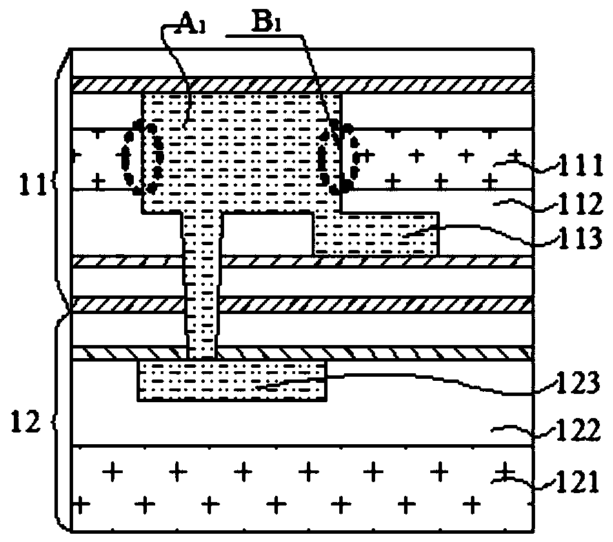
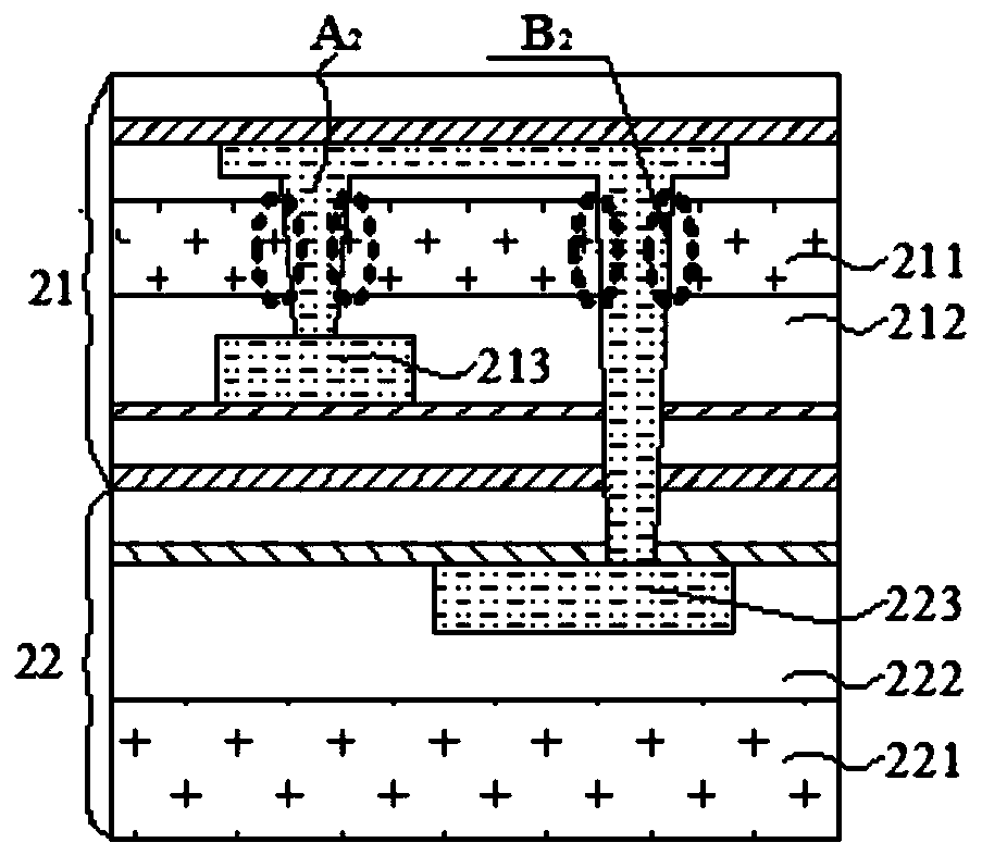
[0060] The auxiliary metal layer 316 has a cross-sectional shape parallel to the first substrate 311 (transverse direction), and its cross-sectional shape is any one of circular rings, square rings, or square arrays distributed at intervals, where the squares include rectangles and squares. The shape of the opening V corresponds to the shape of the auxiliary metal layer. Example 1: The transverse cross-sectional shape of the auxiliary metal layer is a circular ring, the transverse cross-sectional shape of the opening is circular, the opening exposes the annular inner wall of the auxiliary metal layer, and the auxiliary metal layer is The height in the Z direction is h, the cross-sectional shape of the layer where the auxiliary metal layer is located is circular (for example, the radius is a), and the side area of ​​the auxiliary metal layer exposed by the opening is S=2πah. Example 2: The transverse cross-sectional shape of the auxiliary metal layer is a square ring, and the t...


PUM


Abstract

The invention provides a semiconductor device and a manufacturing method thereof. The semiconductor device comprises at least one auxiliary metal layer, wherein the auxiliary metal layer is located between a first metal layer to be interconnected and a second metal layer to be interconnected; the side surface of the auxiliary metal layer is exposed by an opening; the area of the exposed metal layer is increased, so that the filling rate of the interconnection layer from the bottom of the opening to the top is increased, the bottom of the opening is filled as soon as possible to form the interconnection layer, and interconnection failure caused by advanced sealing of the top in the interconnection layer filling process is avoided. The top surface of the interconnection layer is lower than the surface of a first substrate close to one side of the interconnection layer; and the interconnection layer is not formed between the penetrating first substrates, so that insulation between the interconnection layer and the first substrates is ensured, the wiring distance between the first metal layer to be interconnected and the second metal layer to be interconnected is reduced, and the wiring capacitance is also reduced at the same time.

Description

technical field [0001] The invention belongs to the technical field of integrated circuit manufacturing, and in particular relates to a semiconductor device and a manufacturing method thereof. Background technique [0002] Under the trend of highly integrated semiconductor development, the integration of chips with different functions is the main development direction of semiconductor packaging technology. Wafer-level stacking based on 3D-IC technology can achieve lower cost, faster and higher density. Target. After wafer bonding, how to realize the metal interconnection between wafers is an important process in the semiconductor process. [0003] figure 1 It is a metal interconnection structure diagram between stacked wafers. The upper wafer 11 and the lower wafer 12 are stacked and bonded. The upper wafer 11 includes an upper wafer substrate 111, an upper wafer dielectric layer 112 and an upper wafer. Round metal layer 113, lower wafer 12 includes lower wafer substrate ...

Claims


Application Information

Patent Timeline
Patent Type & Authority Applications(China)
IPC IPC(8): H01L23/535H01L23/48H01L21/768
CPCH01L21/76877H01L21/76895H01L23/481H01L23/535
Inventor 叶国梁占迪宋胜金
Owner WUHAN XINXIN SEMICON MFG CO LTD
Why Eureka
Try Eureka