Molybdenum burning bowl and semiconductor ceramic semiconducting process

A semiconducting and semiconducting technology, applied in the field of semiconducting ceramics, to achieve the effect of improving process adaptability, high strength, and no peeling

Pending Publication Date: 2020-09-04
SHAANXI HUAXING ELECTRONICS DEV
View PDF0 Cites 1 Cited by
  • Summary
  • Abstract
  • Description
  • Claims
  • Application Information

AI Technical Summary

Problems solved by technology

[0016] Aiming at the problems existing in the existing firing pots, the present invent

Method used


Image

  • Molybdenum burning bowl and semiconductor ceramic semiconducting process
  • Molybdenum burning bowl and semiconductor ceramic semiconducting process

Examples


Embodiment Construction

[0038] In order to make the purposes, technical solutions and advantages of the embodiments of the present application clearer, the technical solutions in the embodiments of the present application will be clearly and completely described below in conjunction with the drawings in the embodiments of the present application. Obviously, the described embodiments It is a part of the embodiments of this application, not all of them. Based on the embodiments in this application, all other embodiments obtained by persons of ordinary skill in the art without creative efforts fall within the protection scope of this application.

[0039] Below in conjunction with accompanying drawing, technical scheme of the present invention is described in detail:

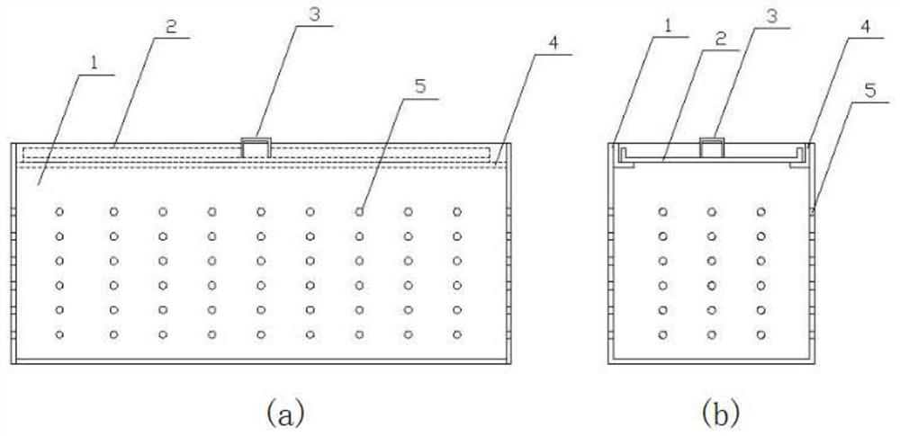
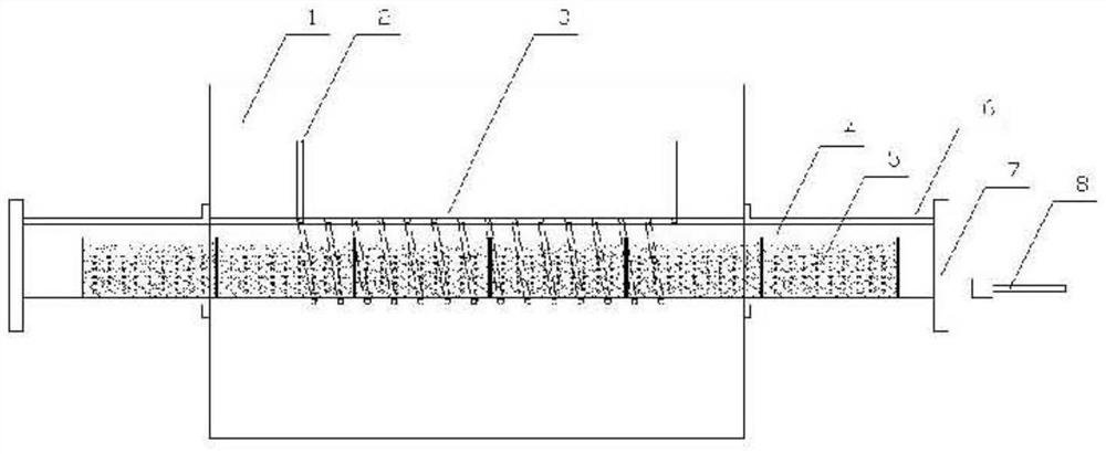
[0040] figure 1 It is an outline drawing of the molybdenum firing pot of the present invention, and the firing pot of the semiconductor ceramic semiconducting process is made of metal molybdenum in the present invention. Specifically, t...


PUM

PropertyMeasurementUnit
Edge thicknessaaaaaaaaaa

Abstract

The invention provides a molybdenum burning bowl and a semiconductor ceramic semiconducting process. The molybdenum burning bowl is of a cuboid structure, wherein three rows of air holes are evenly formed in the two side faces in the length direction. The semiconductor ceramic semiconducting process comprises the following steps that a closed furnace body is filled with 75% H2 + 25% N2 reducing gas, and heating molybdenum wires are electrified to heat the molybdenum wires to 1000-1100 DEG C; the molybdenum burning bowl is filled with products to be reduced, a furnace door on one side of the closed furnace body is opened on the premise of ensuring safety, and the molybdenum burning bowl is conveyed into a high-temperature-resistant furnace tube in the closed furnace body through a pushing mechanism for semi-conduction. Molybdenum has the characteristics of no deformation in a high-temperature reducing atmosphere, high temperature resistance, no discoloration in a reducing atmosphere, nopeeling and high strength, so that Al2O3 and a stainless steel burning bowl are replaced by the molybdenum burning bowl in the semiconductor ceramic semiconducting process, the process adaptability is obviously improved, and the economical efficiency of the molybdenum burning bowl is higher for a long time.

Description

technical field [0001] The invention belongs to the technical field of semiconductor ceramics, and relates to a high-temperature semiconducting process in a reducing atmosphere during the production of surface-type semiconductor ceramics, in particular to a molybdenum firing pot and a semiconducting process for semiconducting ceramics. Background technique [0002] The main crystal phase of surface-type semiconducting ceramic capacitors is BaTiO 3 For Class II porcelain as the base material, a small amount of Sr, Ca, Pb and other elements replace Ba at the A site; Zr, Sn and other elements replace Ti at the B site. It is mainly used to adjust the temperature coefficient, that is, to move the Curie temperature. So it basically belongs to barium titanate porcelain. In addition, there may be a small amount of Nb in the porcelain 2 o 3 , La 2 o 3 Impurities such as donors and sintering accelerators such as AST. A small amount of CuO, Fe 2 o 3 , MnO 2 etc. as acceptor i...

Claims


Application Information

Patent Timeline
IPC IPC(8): F27D5/00H01G4/12
CPCF27D5/0012H01G4/1272
Inventor 蒋小明
Owner SHAANXI HUAXING ELECTRONICS DEV
Why Eureka
Try Eureka