Design method and system for reducing link loss of circuit board, and circuit board

A link loss and design method technology, applied in printed circuit components, computer-aided design, programmable/customizable/modified circuits, etc., can solve the problem of increased circuit board cost, occupied circuit board space, and increased circuit board cost High-level problems, to prevent circuit board delamination problems, reduce link loss, and avoid cost increases

Pending Publication Date: 2020-09-11
LANGCHAO ELECTRONIC INFORMATION IND CO LTD
View PDF8 Cites 3 Cited by
  • Summary
  • Abstract
  • Description
  • Claims
  • Application Information

AI Technical Summary

Problems solved by technology

However, the driver chip also leads to an increase in the cost of the circuit board, especially when more links need to be added to the driver chip, the cost of the circuit board is significantly increased; in addition, the driver chip and its peripheral circuits need to occupy a certain amount of space on the circuit board, which not only increases the number of circuits Difficulty routing the board and is not conducive to board designs with small spaces

Method used


Image

  • Design method and system for reducing link loss of circuit board, and circuit board
  • Design method and system for reducing link loss of circuit board, and circuit board
  • Design method and system for reducing link loss of circuit board, and circuit board

Examples


Embodiment Construction

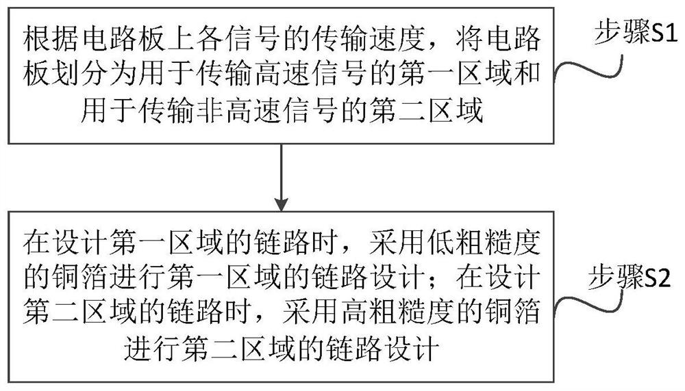
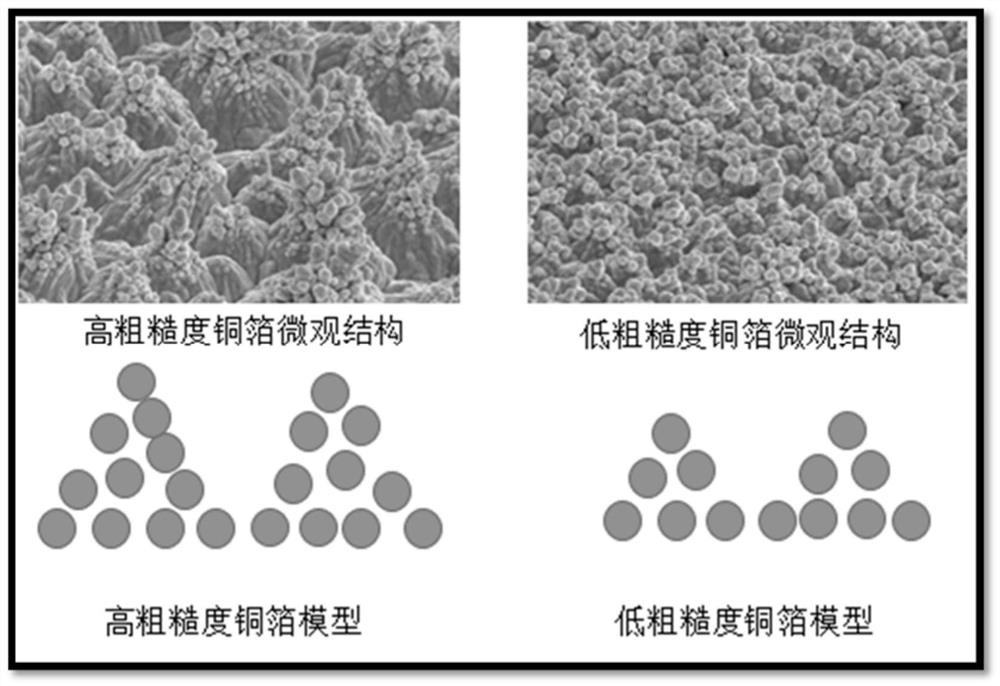
[0048] The core of the present invention is to provide a design method, system and circuit board for reducing the link loss of the circuit board. The link loss is reduced by reducing the roughness of the link copper foil, and the cost increase caused by upgrading the circuit board is avoided. problem and the problem of insufficient wiring space caused by additional driver chips; moreover, this application only reduces the copper foil roughness of high-speed signal links with high link loss requirements, and the copper foil roughness of non-high-speed signal links remains high. Roughness, in order to ensure the degree of bonding between the copper foil and the interlayer medium of the circuit board on the basis of meeting the circuit board link loss requirements, so as to prevent the problem of circuit board delamination caused by insufficient bonding.

[0049] In order to make the purpose, technical solutions and advantages of the embodiments of the present invention clearer, t...


PUM


Abstract

The invention discloses a design method and system for reducing link loss of a circuit board, and the circuit board. According to the method, a circuit board is divided into a first area for transmitting high-speed signals and a second area for transmitting non-high-speed signals; when the link of the first area is designed, low-roughness copper foil is adopted to design the link of the first area; and when the link of the second area is designed, the link of the second area is designed by adopting the copper foil with high roughness. According to the invention, the link loss is reduced by reducing the roughness of the copper foil of the link, so that the problems of cost increase caused by upgrading of the circuit board and insufficient wiring space caused by additional arrangement of thedriving chip are avoided; and only the copper foil roughness of the high-speed signal link with high link loss requirement is reduced, and the roughness of the copper foil of the non-high-speed signal link still maintains high roughness, so that the bonding degree of the copper foil and the interlayer dielectric of the circuit board is ensured on the basis of meeting the link loss requirement ofthe circuit board so as to prevent the problem of circuit board layering caused by insufficient bonding.

Description

technical field [0001] The invention relates to the field of circuit board design, in particular to a design method, system and circuit board for reducing circuit board link loss. Background technique [0002] In the process of link design on the circuit board, link loss is an important factor affecting link signal quality, so optimizing link loss is particularly important. At present, in the link design, there are two commonly used link loss reduction methods for the problem of excessive link loss: 1) Improve the board material grade of the circuit board to use the circuit board material with lower loss to reduce the link loss. loss. However, the cost of circuit boards with high board grades is relatively high, especially when only some links on the circuit board have high loss requirements, it is wasteful to upgrade the board for the entire circuit board. 2) Add a driver chip in the link to enhance the signal strength in the link to offset the loss of the signal in the l...

Claims


Application Information

Patent Timeline
Patent Type & Authority Applications(China)
IPC IPC(8): H05K1/02G06F30/398G06F30/394
CPCH05K1/0286G06F30/398G06F30/394
Inventor 荣世立李岩
Owner LANGCHAO ELECTRONIC INFORMATION IND CO LTD
Why Eureka
Try Eureka