Unlock instant, AI-driven research and patent intelligence for your innovation.

Reverse conducting IGBT device

A reverse-conducting device technology, applied in the field of power semiconductor devices, can solve the problems of large local power consumption, local concentration of current, device burnout, etc., and achieve the effect of eliminating the snap-back phenomenon

Inactive Publication Date: 2020-09-22
UNIV OF ELECTRONIC SCI & TECH OF CHINA
View PDF3 Cites 2 Cited by
  • Summary
  • Abstract
  • Description
  • Claims
  • Application Information

AI Technical Summary

Problems solved by technology

Since the conduction mode changes from the unipolar MOSFET conduction mode to the bipolar IGBT conduction mode, the conductance modulation effect will cause the on-resistance to drop rapidly, resulting in the snap-back phenomenon
The snap-back phenomenon can easily cause local current concentration in the IGBT module, which further leads to excessive local power consumption and burns out the device

Method used


Image

  • Reverse conducting IGBT device
  • Reverse conducting IGBT device
  • Reverse conducting IGBT device

Examples


Embodiment 1

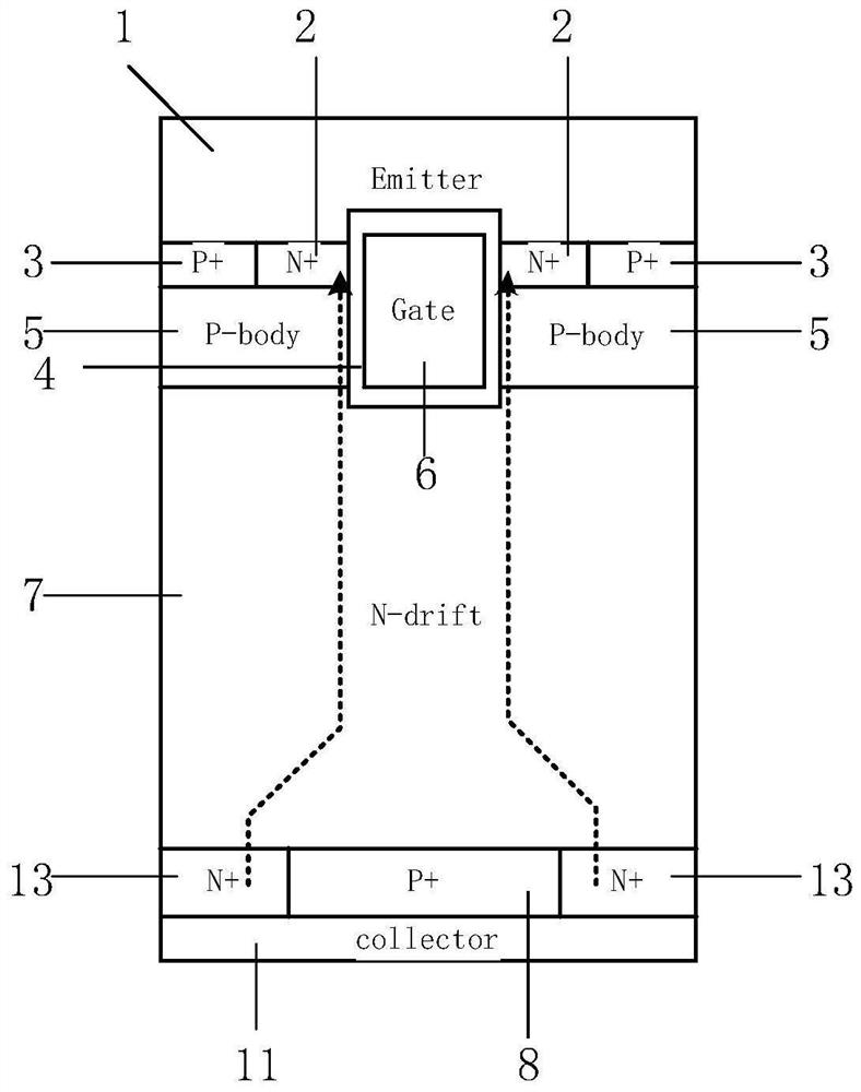
[0022] Such as image 3 As shown, a reverse conduction type IGBT device includes an emitter metal 1, a heavily doped second conductivity type semiconductor emitter region 2, a heavily doped first conductivity type semiconductor ohmic contact region 3, a moderately doped first conductivity type semiconductor Body region 5, polysilicon gate electrode 6, gate insulating oxide layer 4, lightly doped second conductivity type semiconductor drift region 7, heavily doped first conductivity type semiconductor collector region 8, heavily doped first conductivity type semiconductor diode Region 9, heavily doped second conductivity type semiconductor diode region 10, collector metal 11;

[0023]The two sides of the polysilicon gate electrode 6 are heavily doped second conductivity type semiconductor emission regions 2, and the side of the heavily doped second conductivity type semiconductor emission region 2 away from the polysilicon gate electrode 6 is heavily doped first conductivity ty...

Embodiment 2

[0031] Such as Figure 5 As shown, the difference between this embodiment and Embodiment 1 is that a moderately doped second conductive type is provided between the lower surface of the lightly doped second conductive type semiconductor drift region 7 and the heavily doped second conductive type semiconductor diode region 10. type semiconductor field stop region 12 , the lower surface of the second conductivity type semiconductor field stop region 12 is in direct contact with the first conductivity type semiconductor collector region 8 and the heavily doped second conductivity type semiconductor diode region 10 .

[0032] The introduction of the second conductivity type semiconductor field stop region 12 can further optimize the compromise relationship between the forward conduction voltage drop and the reverse withstand voltage of the reverse conduction type IGBT.

[0033] The reverse conduction IGBT device proposed by the present invention is also suitable for devices made o...


PUM


Abstract

The invention relates to the technical field of power semiconductor devices, and particularly relates to a reverse conducting IGBT device. According to the invention, on the basis of a traditional reverse-conducting IGBT device, an N-region doped region of a collector structure is replaced by a diode composed of a heavily-doped N region and a heavily-doped P region which are arranged longitudinally; the doping concentrations of the heavily doped N region and P region are controlled; the built-in potential of the diode reaches the forbidden band width; the diode can play a follow current role by utilizing tunneling current when the IGBT is reversely blocked, and when the reverse conducting IGBT is in a forward conducting state, the device does not have a parasitic VDMOS structure, so that the snap-back phenomenon of the reverse conducting IGBT device is eliminated.

Description

technical field [0001] The invention relates to the technical field of power semiconductor devices, in particular to a reverse conduction insulated gate bipolar transistor (IGBT). Background technique [0002] IGBT (Insualated Gate Biporlar Transistor), insulated gate bipolar transistor, is a composite device composed of MOSFET (insulated gate field effect transistor) and BJT (bipolar transistor), which also has simple gate drive of MOSFET , the advantages of fast turn-on speed and the advantages of large current-carrying density and low on-resistance under BJT conduction, so it is widely used in various high-power power systems. [0003] When IGBT is used as a switching device to process high-power signals, since there are only parasitic transistors inside it, and there is no internal parasitic diode like MOSFET, it is necessary to configure an anti-parallel diode with the same withstand voltage for each IGBT device. As a freewheeling diode. In order to reduce the process...

Claims


Application Information

Patent Timeline
IPC IPC(8): H01L29/739H01L29/06H01L27/07
CPCH01L27/0727H01L29/0603H01L29/0684H01L29/7397
Inventor 任敏李吕强蓝瑶瑶郭乔李泽宏张波
Owner UNIV OF ELECTRONIC SCI & TECH OF CHINA