VDMOS device with high avalanche tolerance and preparation method

An avalanche tolerance and device technology, applied in semiconductor/solid-state device manufacturing, semiconductor devices, electrical components, etc., can solve the problems of inability to completely eliminate parasitic BJT turn-on, device failure, etc., to improve forward conduction characteristics and improve UIS resistance. Effect

Inactive Publication Date: 2020-09-22
UNIV OF ELECTRONIC SCI & TECH OF CHINA
View PDF6 Cites 2 Cited by
  • Summary
  • Abstract
  • Description
  • Claims
  • Application Information

AI Technical Summary

Problems solved by technology

[0004] Usually, the industry often uses reducing the resistance of the body region to suppress the turn-on of the parasitic BJT, but this method cannot completely prevent the turn-on of the parasitic BJT, and the device will still face various fail

Method used


Image

  • VDMOS device with high avalanche tolerance and preparation method
  • VDMOS device with high avalanche tolerance and preparation method
  • VDMOS device with high avalanche tolerance and preparation method

Examples


Embodiment 1

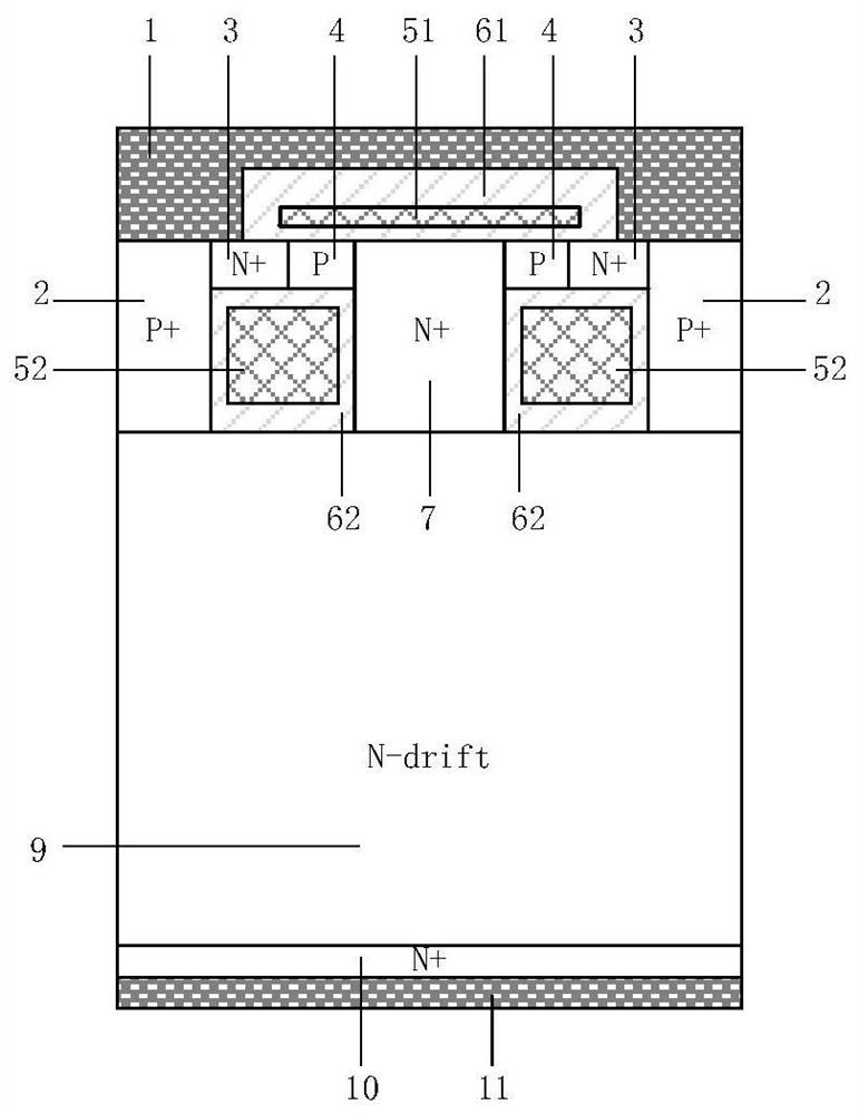
[0050] A high avalanche withstand VDMOS device, the structure of which is as figure 2 As shown, including drain structure, drift region structure, JEFT region structure, source structure, gate structure;

[0051] The drain structure includes a drain metal layer 11, a heavily doped second conductivity type semiconductor drain region 10 above the drain metal layer 11, the lower surface of the heavily doped second conductivity type semiconductor drain region 10 and the drain The metal layer 11 is in direct contact;

[0052] The drift region structure includes a lightly doped second conductivity type semiconductor drift region 9 above the second conductivity type semiconductor drain region 10; the lower surface of the lightly doped second conductivity type semiconductor drift region 9 is heavily doped The doped semiconductor drain region 10 of the second conductivity type is in direct contact with, and the lightly doped semiconductor drift region 9 of the second conductivity typ...

Embodiment 2

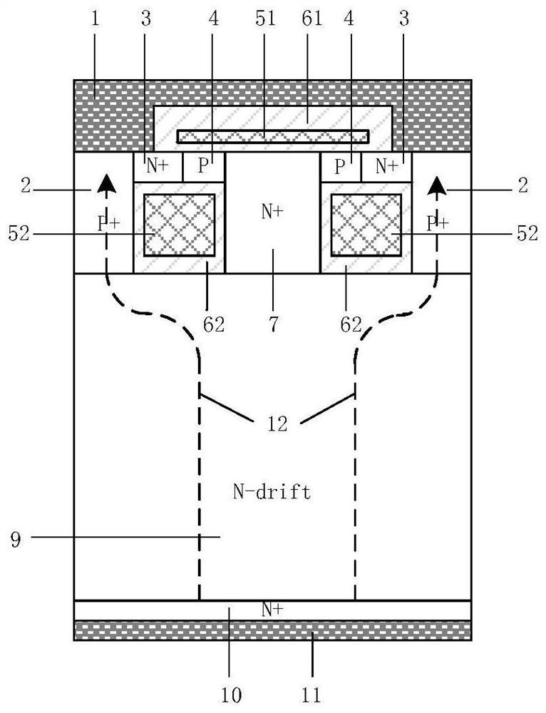
[0076] Based on the structure of Example 1, the structure of this example replaces the lightly doped semiconductor drift region structure of the second conductivity type with a super junction structure, such as Figure 4As shown, the drift region is alternately arranged with lightly doped semiconductor drift regions 8 of the first conductive type and semiconductor regions 9 of lightly doped second conductive type with the same width and doping concentration, so that a high The avalanche-resistant double-channel super-junction VDMOS can further reduce the on-resistance of the device and obtain a higher blocking voltage compared with Example 1.


PUM


Abstract

The invention relates to the technical field of power semiconductor devices. The invention relates to a VDMOS with improved avalanche tolerance and a preparation method. According to the invention, asecond polysilicon gate electrode is introduced into the device to replace part of abody region underasource region of atraditional VDMOS structure; aJEFT region is subjected to medium doping with thesame impurity type as adrift region; when the device is in forward conduction, afirst polysilicon gate electrode and the second polysilicon gate electrode can form a double-inversion-layer channel inthe body region inthe side part of the source region, and an accumulation layer of majority carriers is formed in the JEFT region, so that the forward conduction characteristic of the VDMOS is improved; when the device is in an avalanche breakdown state, there is no parasitic triode under the source region any more, the breakdown position can be fixed to the interface of anohmic contact region onthe side of the source region and the drift region, avalanche current can only flow out of the source electrode through the ohmic contact region, and the avalanche tolerance of the VDMOS is improved.

Description

technical field [0001] The invention relates to the technical field of power semiconductor devices, in particular to a VDMOS with high avalanche tolerance and its preparation. Background technique [0002] Insulated gate field effect transistor (MOSFET) is widely used in various power systems because of its advantages of fast switching speed, low power consumption, easy gate drive, low drive power, high input impedance and good frequency response. In various high electrical stress systems, in addition to requiring lower conduction losses of power MOSFETs, higher reliability is also required. Generally, power MOSFETs often face failure in the dynamic process. The difference from failure in the static process is that the probability of device failure in the dynamic process is higher, and the failure mechanism is more complicated. The unclamped inductive load switching process (Unclamped InductiveSwitching, UIS) is generally considered to be the most extreme electrical stress ...

Claims


Application Information

Patent Timeline
IPC IPC(8): H01L29/78H01L29/06H01L21/336
CPCH01L29/0619H01L29/0634H01L29/0684H01L29/66068H01L29/66712H01L29/7811H01L29/7831
Inventor 任敏李吕强蓝瑶瑶郭乔李泽宏张波
Owner UNIV OF ELECTRONIC SCI & TECH OF CHINA
Why Eureka
Try Eureka